


Description
This reference design is a 15-W bias power supply with two isolated outputs (12 V/1.125A and 3.3 V/0.3A) and a total standby power consumption of 4 mW under a 220-V AC input. The controller uses primary-side regulation (PSR) and detects a wake-up signal from the UCC24650 secondary-side voltage-droop monitor for improved transient response to large load steps. This reference design demonstrates how the UCC28730 can provide ultra-low standby power without sacrificing start-up time or output transient response with an internal 700-V start-up switch, dynamically controlled operating states, and a tailored modulation profile. The UCC28730 uses frequency modulation, peak primary current modulation, valley switching, and valley skipping in its control algorithm to maximize efficiency over the entire operating range.


 Features
- Enables Zero-Power Standby Consumption, 3.1 mW at 115-V AC Input and 4.2 mW at 220- V AC Input
- Average Efficiency > 84%, Exceeds DoE VI and CoC Tier 2 Specifications
- Primary-Side Regulation (PSR) Eliminates Optocoupler and Increase Reliability of Bias Power Supply
- Resonant-Ring Valley-Switching Operation for Highest Overall Efficiency
- Universal Input Voltage Range (85-V to 270-V AC) to Address Customer Needs Across All Regions
- Dual Isolated Outputs of 12 V and 3.3 V is Suitable for Most Industry Applications
- Frequency-Dither to Ease EMI Compliance
- Full Protection With Overvoltage, Low-Line, and Overcurrent Functions
Applications
- Washing Machines
- Coffee Machines
- Cooking Ranges
- Small Home Appliances
- Disinfection Cabinets
- Toilet Seat Covers
- TV and Monitor Power Supplies
 1 System Description
The International Electrotechnical Commission (IEC) specifies methods of measurement of electrical power consumption in standby modes and other low power modes (off mode and network mode), as applicable in IEC 62301:2011. These methods are applicable to electrical products with a rated input voltage or voltage range that lies wholly or partly in the range of 100-V to 250-V AC for single-phase products and 130-V to 480-V AC for other products. Clause 4.5 of this standard regards measurements of less than 5 mW as zero power, which now has become the basis for a “Zero Power” marketing campaign as the ultimate target for no-load standby dissipation in electronic devices and appliances. Products that meet this requirement can earn a “Zero Power” label.
Most of industrial applications need a bias power supply and at least has dual power rails for the entire system: 3.3 V or 5 V for the system controller and 12 V or 15 V for the power module. This reference design provides dual isolated outputs of 3.3 V and 12 V that cover most industrial applications. This design also achieves very low power consumption in standby mode: 3-mW standby power consumption at a 115-V AC input and 4.4 mW at a 230-V AC input. The design is suited for use in isolated off-line systems requiring minimal standby power, high efficiency, and fault protection. Such applications include:
- SMPS for home appliance and building automation
- TVs and monitor power supplies
Adapters and chargers for smartphones, tablets, and consumer electronics
2 System Overview
2.1 Block Diagram
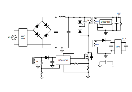
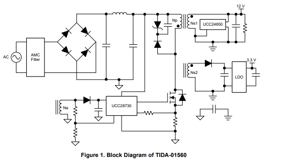
Figure 1 shows the high-level block diagram of the circuit. The main parts of this reference design are the isolated-flyback power supply controller (UCC28730), voltage monitor (UCC24650), and next-generation, low-dropout regulators ( TLV 74333).
 2.2 Design Considerations
IEC 62301:2011 defines “Zero Power” as standby power consumption of a system that is below 5 mW. For different industry applications, the system power level can be from tens to hundreds of watts. Above this power level, the requirement for x-capacitor discharge as well as the parasitic dissipation in the components make it very difficult to achieve zero power. For example, the bulk capacitor leakage current can amount to several mW at high line input. To enable zero power for higher power designs, the UCC24650 features an output enable pin, which can drive a relay to disconnect the AC input voltage at a very light load and reduce power dissipation to below 5 mW.
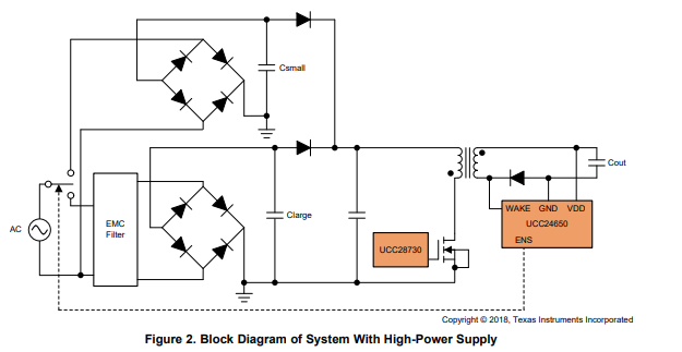
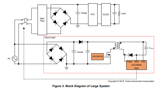
Based on this operating principle, this reference design has two options to help achieve the zero standby power for different applications: high-power supply system (Figure 2) and larger system (Figure 3).
Figure 2 shows a block diagram of a system with a high-power supply. During normal operation mode, this system operates with a large capacitor of a larger leakage current and a full EMI filter. During standby mode, ENS of the UCC24650 switches the relay and lets the system operate with a small capacitor of much less leakage current and without EMI filter.
Figure 3 shows a block diagram of a large system. Usually, a large system is supplied as several portions, just like power factor correction (PFC), DC/DC converter, DC/AC inverter, and so on. During normal operation mode, zero standby power flyback serves as the auxiliary power supply for the system. During standby mode, ENS of the UCC24650 shuts off the relay and only the flyback is connected to the power line, making it easy to achieve zero standby power.
 2.3 Highlighted Products
This reference design features the following devices, which are selected based on their specifications. For more information on each of these devices, see their respective product folders at TI.com or click on the links for the product folders under Resources.
2.3.1 UCC28730
The UCC28730 is an isolated-flyback power supply controller that provides accurate voltage and constant current regulation using primary-side winding sensing, eliminating the need for optocoupler feedback circuits. The controller operates in discontinuous conduction mode with valley switching to minimize switching losses. The modulation scheme is a combination of frequency modulation and primary peakcurrent modulation to provide high conversion efficiency across the load range. The control law provides a wide dynamic operating range of output power, which facilitates the achievement of <5-mW standby power.
During low-power operating levels, the device has power management features to reduce the device operating current at switching frequencies less than 28 kHz. The UCC28730 includes features in the pulse-width modulator to reduce the EMI peak energy at the fundamental switching frequency and its harmonics. Accurate voltage and current regulation, fast dynamic response, and fault protection are achieved with primary-side control. A complete charger solution can be realized with a straightforward design process, low cost, and low component count.
1.1.1 UCC24650
The UCC24650 is a voltage monitor designed to alert a companion primary-side controller device when the monitor detects a relative droop of approximately 3% on its VDD input. Commonly known as a wakeup device, the UCC24650 is normally used in isolated-flyback power supply applications using primaryside regulation (PSR). Because the PSR controller can operate at very low frequencies during light-load or no-load conditions, the controller cannot detect a sudden load step that can occur between power cycles, and the output voltage can fall out of regulation. The UCC24650 can detect the voltage droop and wakeup a compatible PSR controller to increase its switching frequency before the output falls too low. This action significantly reduces the amount of output capacitance needed to achieve an acceptable transient response.
At the end of each power cycle delivered by the PSR controller, the UCC24650 droop monitor refreshes an internally stored voltage scaled to 97% of the VDD voltage. If the monitor detects a droop of VDD to the level of the stored voltage, the WAKE signal is connected to GND by an internal low-impedance switch. The WAKE signal transmits a current pulse across the isolation transformer to a compatible PSR controller, such as the UCC28730, capable of detecting the wake-up signal on the primary side of the transformer.
The UCC24650 is also capable of disabling a compatible PSR controller, such as the UCC24610, during light-load conditions to minimize standby power. The ENS output signal is driven low after a fixed sustained count of low-frequency power pulses and can re-enable the PSR controller after a cumulative count of 32 higher-frequency power pulses. The ENS output can also be used to drive other secondary circuitry compatible with the ENS operating parameters.
1.1.2 TLV74333
The TLV74333 device belongs to a new family of next-generation, low-dropout regulators (LDOs). This device consumes low quiescent current and delivers excellent line and load transient performance. Combined with low noise, good PSRR, and low-dropout voltage, these characteristics make this device well-suited for portable consumer applications.
This regulator offers foldback current limit, shutdown, and thermal protection. The operating junction temperature for this device is –40°C to +125°C.
2.4 System Design Theory
This reference design uses the UCC28730 controller with the UCC24650 wake-up monitor in a 15- W converter to provide dual isolated outputs of 12 V with 1.125 A and 3.3 V with 0.3 A. The input accepts an universal voltage range of 85-V to 265-V AC.
Depending upon the operating conditions, the control law algorithm modulates the switching frequency or the peak primary current to satisfy the power transfer requirements. As the load is increased from zero, the converter transitions through a frequency modulation (FM) mode. The peak primary current is held constant at one-third of its full-load peak value as the switching frequency increases from a minimum value to maintain energy transfer up to 28 kHz. When the load is increased to the level at which the switching frequency reaches 28 kHz, the controller keeps the switching frequency fixed and modulates the amplitude of peak primary current, increasing it from one-third its peak value up to its maximum full load peak current value; this area of operation is referred to as the amplitude modulation (AM) range. A further increase in load demand transitions the controller into another FM mode where the peak primary current is constant at its maximum designed value and the switching frequency is increased as needed, up to the maximum switching frequency of the controller (83 kHz).
Using PSR, the output voltage is indirectly sensed on the auxiliary winding once the stored transformer energy is transferred to the secondary to maintain a tightly regulated output. The wake-up monitoring feature operates in conjunction with the secondary-side UCC24650 to allow light-load and no-load switching frequencies to approach 32 Hz. This controller minimizes no-load power consumption to less than 5 mW while providing a fast dynamic response to load transients without requiring large output capacitance. The controller further enhances its efficient operation with valley switching. The UCC28730 also uses dithering of the gate drive, which helps to ease EMI compliance. This design guide provides the schematic, component list, assembly drawing, and test setup necessary to evaluate the UCC28730 and UCC24650 in a typical off-line converter application.
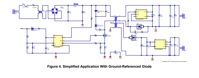
A typical application for the UCC28730 controller includes the compatible UCC24650 wake-up monitor to regulate an isolated low-voltage DC output with low output capacitance. When the UCC28730 is operating in the low-frequency wait state, the UCC24650 alerts the UCC28730 to a sudden load increase, avoiding the need for extremely high output capacitance to hold up between power cycles. As shown in Figure 4, the output rectification uses a ground-referenced diode to facilitate application of the UCC24650 device. A ground-referenced synchronous rectifier can also be used.
 2.4.1 Wake-Up Detection and Function
A major feature available at the VS pin of the UCC28730 is the wake-up function, which operates in conjunction with a companion secondary-side wake-up device, such as the UCC24650. This feature allows light-load and no-load switching frequencies to approach 32 Hz to minimize losses, yet wake the UCC28730 from its wait state (sleep mode) in the event of a significant load step between power cycles. Despite the low frequencies, excessive output capacitance is not required to maintain reasonable transient response. While in the wait state, the UCC28730 continually monitors the VS input for a wake-up signal and, when detected, responds immediately with several high-frequency power cycles and resumes operation as required by the control law to recover from the load-step transient and restore output voltage regulation.
Because the wake-up feature interrupts the wait state between very low frequency switching cycles, the feature allows the use of a much lower output capacitance value than would be required to hold up the voltage without the wake-up function. The feature also allows the controller to drop to extremely low switching frequencies at no-load conditions to minimize switching losses. This drop facilitates the achievement of less than 5 mW of input power to meet zero-power standby requirements. The UCC28730 controller alone cannot ensure zero-power operation because other system-level limitations are also imposed; however, the UCC28730 and UCC24650 together make this goal achievable.
2.4.2 Valley Switching and Valley Skipping
The UCC28730 uses valley-switching to reduce switching losses in the MOSFET, to reduce induced-EMI, and to minimize the turnon current spike at the current sense resistor. The controller operates in valley switching in all load conditions unless the VDS ringing is diminished to the point where valleys are no longer detectable.
Valley skipping modulates each switching cycle into discrete period durations. During FM operation, the switching cycles are periods when energy is delivered to the output in fixed packets, and the power delivered varies inversely with the switching period. During operating conditions when the switching period is relatively short, such as at high-load and low-line, the average power delivered per cycle varies significantly based on the number of valleys skipped between cycles. As a consequence, valley skipping adds additional low-amplitude ripple voltage to the output with a frequency dependent upon the rate of change of the bulk voltage. For a load with an average power level between that of cycles with fewer valleys skipped and cycles with more valleys skipped, the voltage control loop modulates the control law voltage and toggles between longer and shorter switching periods to match the required average output power.
2.4.3 Fault Protection
The UCC28730 provides comprehensive fault protection. The protection functions include:
- Output overvoltage
- Input undervoltage
- Internal overtemperature
- Primary overcurrent fault
- CS pin fault
- VS pin fault
A UVLO reset and restart sequence applies to all fault protection events.
The output overvoltage function is determined by the voltage feedback on the VS pin. If the voltage sample of VS exceeds 4.6 V for three consecutive switching cycles, the device stops switching and the internal current consumption becomes IFAULT, which discharges the VDD capacitor to the UVLO turnoff threshold. After that, the device returns to the start state and a start-up sequence ensues.
Current into the VS pin during the MOSFET on-time determines the line input run and stop voltages. While the VS pin clamps close to GND during the MOSFET on-time, the current through feedback resistor is monitored to determine a sample of VBULK. A wide separation of the run and stop thresholds allows clean start-up and shutdown of the power supply with line voltage. The run-current threshold is 225 μA, and the stop-current threshold is 80 μA. The input AC voltage to run at start-up always corresponds to the peak voltage of the rectified line because there is no loading on CBULK before start-up. The AC input voltage to stop varies with load because the minimum VBULK depends on the loading and the value of CBULK. At maximum load, the stop voltage is close to the run voltage, but at no-load condition, the stop voltage can be approximately 1/3 of the run voltage.
The UCC28730 always operates with cycle-by-cycle primary-peak current control. The normal operating range of the CS pin is 0.74 V to 0.249 V. An additional protection occurs if the CS pin reaches 1.5 V after the leading-edge blanking interval for three consecutive cycles, which results in a UVLO reset and restart sequence.
Normally at an initial start-up, the peak level of the primary current of the first four power cycles is limited to the minimum VCST(min). If the CS input is shorted or held low such that the VCST(min) level is not reached within 4 μs on the first cycle, the CS input is presumed to be shorted to GND and the fault protection function results in a UVLO reset and restart sequence. Similarly, if the CS input is open, the internal voltage is pulled up to 1.5 V for three consecutive switching cycles and the fault protection function results in a UVLO reset and restart sequence.
The internal overtemperature protection threshold is 165°C. If the junction temperature reaches this threshold, the device initiates a UVLO reset cycle. If the temperature is still high at the end of the UVLO cycle, the protection cycle repeats.
Protection is included in the event of component failures on the VS pin. If a complete loss of feedback information on the VS pin occurs, the controller stops switching and restarts.
2.4.4 Input Bulk Capacitance Calculation
Bulk capacitance can consist of one or more capacitors connected in parallel, often with some inductance between them to suppress differential-mode conducted noise. EMI filter design is beyond the scope of this procedure.
First calculate the input capacitor charge time (tch) based on a 40% ripple voltage:
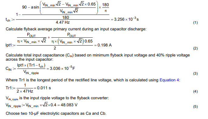
2.4.5 Output Capacitance Calculation
With ordinary flyback converters, the output capacitance value is typically determined by the time of duration, which is defined as 2 ms. Calculate the output capacitance using Equation 6:
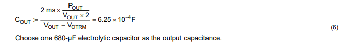
Choose one 680-µF electrolytic capacitor as the output capacitance.
2.4.6 Snubber Circuit Selection
Define the enter voltage of Zener diode as Vz = 150 V.
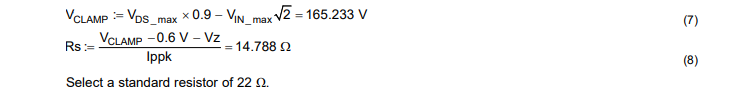 Select a standard resistor of 22 Ω.
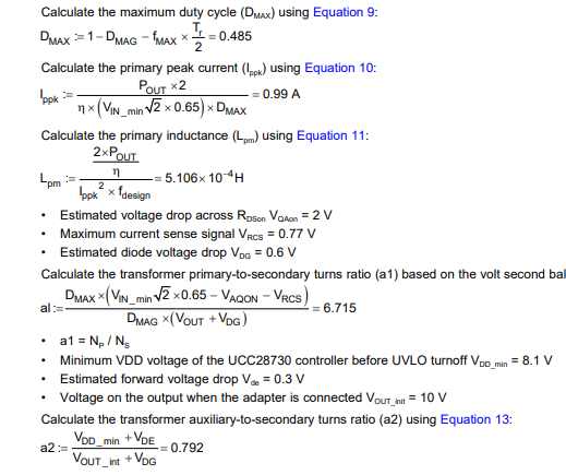
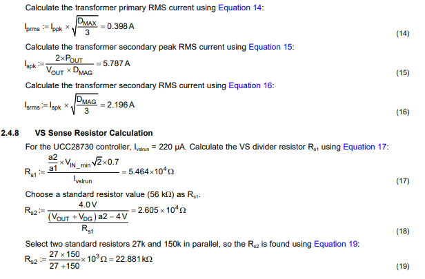
2.4.7 Transformer Design
Define DMAG = 43.2%, where DMAG is the secondary diode of the conduction duty cycle during constant current (CC) operation. In the UCC28730 controller, DMAG is fixed internally at 0.432.
Define Tr = 2 µs, where Tr is the estimated period of the LC tank frequency at the switch node.
3 Hardware, Testing Requirements, and Test Results
3.1 Required Hardware
3.1.1 Test Equipment Needed to Validate Board
- Multimeters: For highest accuracy, VOUT can be monitored by connecting a DC voltmeter; Fluke 287C is recommended.
- Power meter: Use a power analyzer capable of measuring low input current, typically less than 1 mA, and a long integration mode, when low power standby mode input power measurements are taken; WT210 is recommended.
- AC voltage source: For an input source, use an isolated variable AC source capable of supplying between 85-V and 265-V AC at no less than 20 W and connected as shown in Figure 5. For accurate efficiency calculations, insert a power meter between the neutral line of the AC source and the Neutral terminal of the design. For highest accuracy in loaded conditions, connect the voltage terminals of the power meter directly across the Line and Neutral terminals of the design. For highest accuracy at no load, connect the V+ voltage terminal of the power meter at the Line terminal of the design and the V– terminal of the power meter ahead of the shunt resistor; Chroma 61503 is recommended.
- Output load: Use a programmable electronic load capable of sinking 0 A to 3 A. When testing the design in constant current mode, set the electronic load to constant resistance mode; Chroma 63103 is recommended.
- Oscilloscope: A digital or analog oscilloscope with 500-MHz scope probes is recommended; Tektronix DPO 3054 is recommended.
- Wire gauge: The wire connections between the AC source and the design and the wire connections between the design and the load must be less than 2 ft; a wire with a minimum of 18 AWG is recommended.
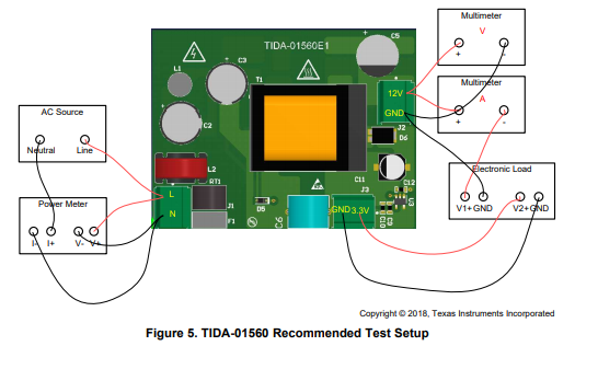
3.1.2 Recommended Test Setup
 3.1.3 Test Procedure
Table 2. Connecter Pin Map
| CONNECTOR | PIN | DESCRIPTION |
| J1 | 1 | Line of AC input |
| 2 | Neutral of AC input | |
| J2 | 1 | 12-V output positive |
| 2 | Ground | |
| J3 | 1 | 3.3-V output positive |
| 2 | Ground |
- Prepare the test setup as shown in Figure 5.
- Connect the line of the AC source on the design input (pin 1 of connector J1), and connect the neutral of the AC source on the TIDA-01560 input (pin 2 of connector J1) through the current sensing module of the power meter.
- Connect the voltage sensing module to the design input (connector J1).
- Connect an electronic load to the 12-V output terminal (connector J2) with the load set to draw 14 W through the multimeter.
- Connect another electronic load to the 3.3-V output terminal (connector J3) with the load set to draw 1 W.
- Turn on the AC source connected to the design input with a universal input voltage (85-V to 264- V AC).
- Once the design activates, monitor the input power consumption and dual output performance.
- Turn off the AC source and disconnect the AC source from the board when the test is complete.
3.2 Testing and Results
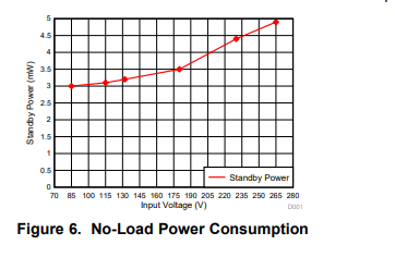
3.2.1 No-Load Power Consumption
No-load power consumption is measured as less than 5 mW over the entire line input range.
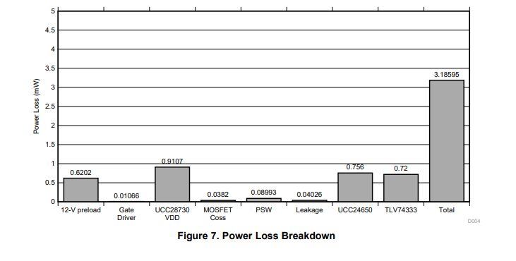
 3.2.2 Power Loss Breakdown (Theoretical Calculation)
This power loss breakdown is based on theoretical calculation, and this calculation does not contain the leakage power loss of the input and output aluminum capacitor.
 3.2.3 Efficiency With Load Variation
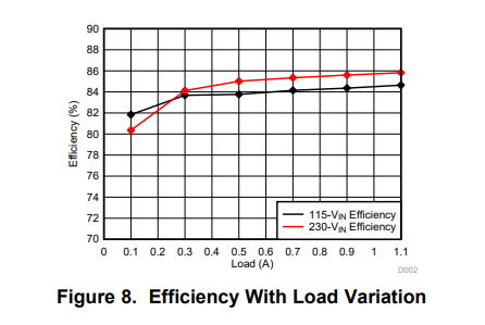 Table 3. Efficiency With Load Variation Under 115-V AC Input
| VIN (V) | PIN (W) | 12 V VOUT (V) | 12 V IOUT (A) | 3.3 VOUT (V) | 3.3 V IOUT (A) | POUT (W) | ƞ ( % ) |
| 115 V | 0.0033 | 12.150 | 0.000 | 3.296 | 0.000 | 0.00 | |
| 1.868 | 12.141 | 0.098 | 3.286 | 0.105 | 1.53 | 81.84 | |
| 4.702 | 12.123 | 0.296 | 3.285 | 0.105 | 3.93 | 83.68 | |
| 7.612 | 12.118 | 0.498 | 3.285 | 0.105 | 6.38 | 83.76 | |
| 10.45 | 12.136 | 0.696 | 3.285 | 0.105 | 8.79 | 84.14 | |
| 13.34 | 12.154 | 0.898 | 3.285 | 0.105 | 11.25 | 84.36 | |
| 16.49 | 12.175 | 1.118 | 3.285 | 0.105 | 13.96 | 84.64 |
Table 4. Efficiency With Load Variation Under 230-V AC Input
| VIN (V) | PIN (W) | 12 V VOUT (V) | 12 V IOUT (A) | 3.3 VOUT (V) | 3.3 V IOUT (A) | POUT (W) | ƞ ( % ) |
| 230 V | 0.0043 | 12.133 | 0.000 | 3.296 | 0.000 | 0.000 | |
| 1.9 | 12.121 | 0.098 | 3.287 | 0.105 | 1.527 | 80.36 | |
| 4.67 | 12.102 | 0.296 | 3.284 | 0.105 | 3.928 | 84.12 | |
| 7.49 | 12.102 | 0.498 | 3.281 | 0.105 | 6.368 | 85.02 | |
| 10.29 | 12.121 | 0.696 | 3.279 | 0.105 | 8.782 | 85.34 | |
| 13.13 | 12.139 | 0.898 | 3.278 | 0.105 | 11.239 | 85.60 | |
| 16.24 | 12.159 | 1.118 | 3.277 | 0.105 | 13.938 | 85.82 |
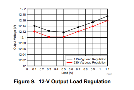
3.2.4 Load Regulation
Figure 9 is the 12-V output load regulation with a fixed 3.3-V/0.1-A output. The load regulation is below 2 %.
 3.2.5 Turnon Waveform
Figure 10 and Figure 11 are start-up waveforms of a 115-V input with no load and full load, respectively.
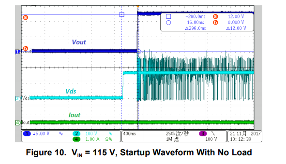
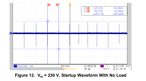
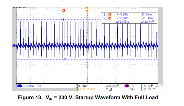
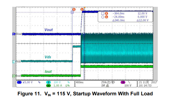 Figure 12 and Figure 13 are start-up waveforms of a 230-V input with no load and full load, respectively.
 3.2.6 Output Voltage Ripple
Figure 14 and Figure 15 show the 12-V output voltage ripple. The measurements are taken at no load and full load with an input voltage of 115-V AC, 50-Hz, and the waveform is AC coupled with a 20- MHz bandwidth limit. The cursor indicates the maximum peak-to-peak limit of 45 mV permitted for the reference design. The ripple pattern seen is characteristic of the EMI dithering method used by the UCC28730 controller.
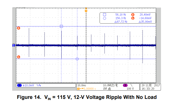
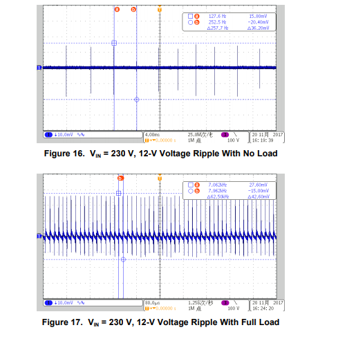
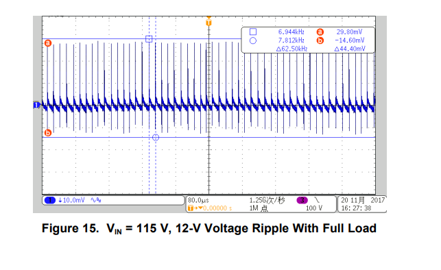 Figure 16 and Figure 17 show the 12-V output voltage ripple. The measurements are taken at no load and full load with an input voltage of 230-V AC, 50-Hz, and the waveform is AC coupled with a 20- MHz bandwidth limit. The cursor indicates the maximum peak-to-peak limit of 45 mV permitted for the reference design. The ripple pattern seen is characteristic of the EMI dithering method used by the UCC28730 controller.
 3.2.7 Transient Response
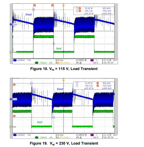
The transient response shown in Figure 18 and Figure 19 are taken with an input voltage of 115-V and
230-V AC, 50-Hz and a load transition from 0 A to full load. Channel 4 is the load current on a scale of 0.5 A per division, and channel 1 is the output voltage on a scale of 200 mV per division, offset from the center line by –12 V. The cursors show the undershoot from the regulated output voltage under full load transient conditions. Output voltage undershoot varies depending on the specific time the transient occurs during the switching cycle.
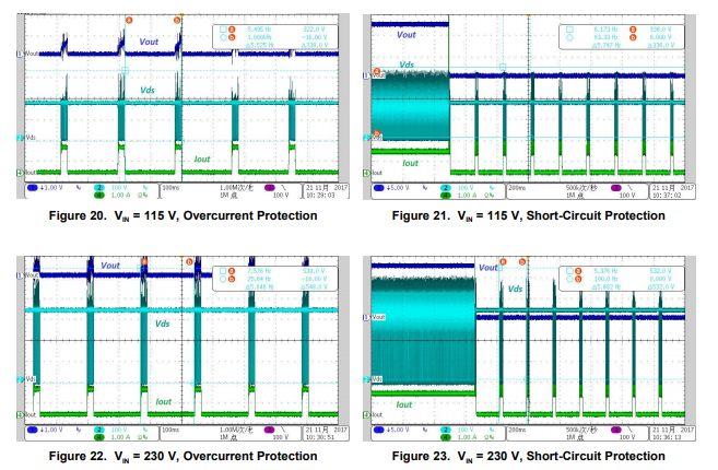
 3.2.8 Overcurrent and Short-Circuit Protection
When UCC28730 go into OCP and SCP conditions, the hiccup frequency is 5.5 Hz, and the output current is limited below 1.3 A.
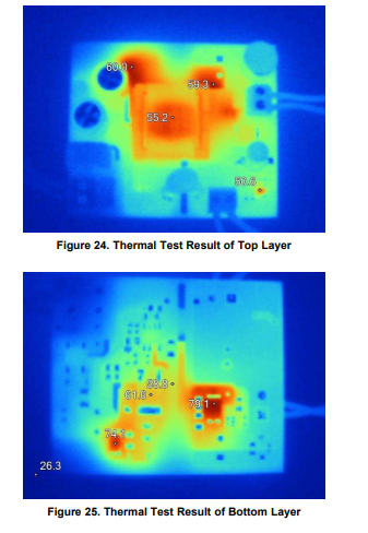
 3.2.9 Thermal Test
Figure 24 and Figure 25 are the thermal test results of the top layer and bottom layer with no force cooling. In each figure, the highest temperature is from the snubber circuit of the primary side.
 3.2.10 EMI Test Result
Figure 26 shows the EMI test setup.
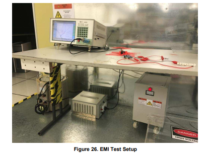 The conducted emissions are compared in a pre-compliance test setup against the EN55022 class B limits and are found to meet the class B limits with ease.
Article Courtesy: Texas Instruments