


Xilinx’s new 16nm and 20nm UltraScale families are based on the first all programmable architecture to span multiple nodes from planar through FinFET technologies and beyond, while also scaling from monolithic through 3D ICs. At 20nm Xilinx pioneered the first ASIC-class All Programmable architecture to enable multi-hundred gigabit-per-second levels of system performance with smart processing at full line rates, scaling to terabits and teraflops. At 16nm, UltraScale+ families combine new memory, 3D-on-3D, and multi-processing SoC (MPSoC) technologies to deliver a generation ahead of value. Giles Peckham, Regional Marketing Director, Xilinx Inc discusses the subject at length with ELE Times. Excerpts.
ELE Times: What are your views on the entry of UltraScale + FPGA, SoC and 3D ICs in the LTE-Advanced, and the wireless 5G.
Giles Peckham: 5G is all about securely connecting billions of devices faster, with a solid connection, almost anywhere. It will go well beyond the current mobile experience, improving overall service to help usher in the era of Internet of Things, with 1000X network capacity for 100X the number of connected devices and machines.


Over 50 billion connected devices are expected by 2020. As a result, 5G networks must be more scalable, intelligent, and heterogeneous. Technologies such as distributed small cells, massive-MIMO with hundreds of antennas, and centralized base-band processing via CloudRAN, will dramatically increase coverage and data throughput. Networks will need to connect securely through backhaul and optical front haul for processing.
For 5G, Xilinx All Programmable technology is helping solve capacity, connectivity, and performance challenges. It also provides the flexibility to support multiple standards, multiple bands and the multiple sub-networks that enable the many diverse IoT driven applications of 5G.
 Xilinx provides a flexible, standards-based solution that combines software programmability, multi-standard and multi-band hardware optimization, and any-to-any connectivity with the security needed for 5G networks. Customers can quickly develop their applications on Zynq MPSoC and UltraScale FPGAs silicon platforms using Vivado High-Level Synthesis, SDSoC, and SDAccel software defined environments.
Xilinx’s products offer customers multiple differentiating advantages vs. other types of solutions. They offer the benefit of a flexible platform that can give them a 1-2 time to market advantage vs. ASIC alternatives at a >50% lower total cost of ownership as well as a scalable future proof platform. The strength of the advanced 16nm process with new technology innovations will allow customers to create architectures that can span 5X the frequency bandwidth at 3X the number of bands traditionally served with ½ the power consumption of older technology solutions.
ELE Times: Define megatrends in Xilinx system design and what are the key challenges?
Giles Peckham: Over 50 Billion devices and machines will be connected by 2020. Once connected, they must be secure to deter intruders, right down to the hardware level. As these devices, machines, systems, and networks become more context aware, they must adapt to their environments and demands, being more programmable and software defined. They also must be scalable, with ever more functions virtualized and efficiently mapped onto shared compute resources. As data and video is captured from sensors and cameras everywhere, analytics must enable these machines to recognize, interpret, decide, and act.
These systems and networks must also meet the growing demands of impatient end users and real time scenarios that require immediate, low latency response. Yet, behind the scenes, they must process an exponentially growing amount of data, packets, and pixels with ever more sophisticated algorithms while consuming the lowest possible power. And they must be highly differentiated, or they will fail in the increasingly competitive and cost sensitive worldwide market. This can only be accomplished by combining software intelligence with hardware optimization and any-to-any connectivity.
Xilinx All Programmable Solutions enable Smarter, Connected, and Differentiated Systems, integrating the highest levels of software-based intelligence with hardware optimization and any-to-any connectivity.
Xilinx is the only company that can enable differentiation through a combination of software intelligence and programmable hardware optimization. All programmable devices with programmable hardware optimization provide 4 differentiating advantages over the type of devices (ASICs, ASSPs, GPUs, CPUs): performance/watt, any to any connectivity, security and safety and chameleon platforms.
ELE Times: How is Xilinx FPGA’ different from the competitors?
Giles Peckham: With an exceptional execution on the 28, 20, and now 16 nanometer nodes, Xilinx has worked hard to maintain three generations of technology leadership. Xilinx is the only PL vendor fully committed to silicon products and solutions for all market segments. Xilinx can simultaneously address today’s 3G, 4G, Pre-5G requirements with our 28, 20, and 16nm products. Our roadmaps are aligned to customer’s 5G development needs since they can leverage our currently shipping 16nm FF+ FinFET based products for early development as well as have confidence in our delivery schedules of future 7nm architectures for their volume production.
Xilinx launched multiple product families with breakthroughs in integration and optimization which has changed the game in price/performance/watt and enabled programmable systems integration. Breakthroughs also include Software Development Environments supporting C, C++ and Open CL development, in particular SDSoC which is the industry’s only C/C++ full-system optimising compiler.
The Xilinx All Programmable product portfolio based on 28nm and 20nm planar and 16Fin FET+ technologies keeps customers a generation ahead of their competition with an expansion of its offerings from three perspectives:
- Portfolio: UltraScale™ architecture-based All Programmable FPGAs, 3D ICs and SoCs
Product: Co-optimized with the Vivado™ Design Suite for extra performance, power, and integration - Productivity: Unmatched time to integration and implementation
Xilinx is committed to staying a generation ahead with aggressive roadmaps across each of the three elements of its broader portfolio, with each element supporting and reinforcing the previous generation. With the addition of UltraScale+, Xilinx has built upon the UltraScale architecture which allows for simple migration between planar and FinFET nodes. This allows customers to migrate their 20nm designs and benefit from the performance per watt advantages of FinFET technology.
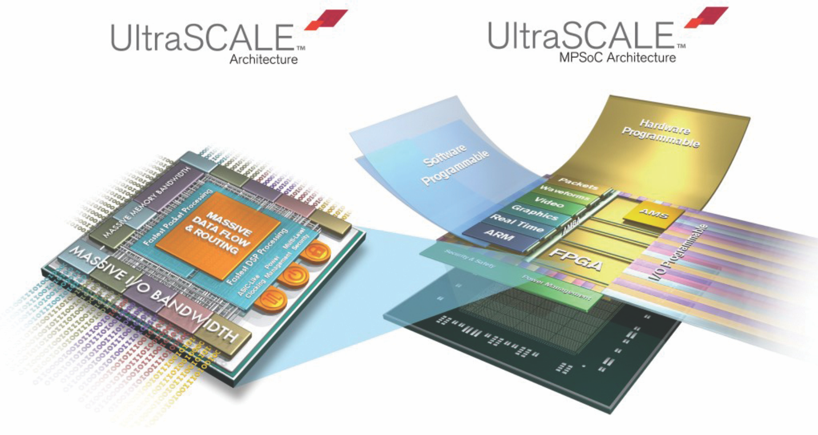
Building on the core UltraScale architecture at 20nm, Xilinx’s 16nm UltraScale+ family of FPGAs, 3D ICs and MPSoCs, combine new UltraRAM and High-Bandwidth Memory (HBM), 3D-on-3D and multi-processing SoC (MPSoC) technologies, delivering a generation ahead of value. To enable the highest level of performance and integration, the UltraScale+ family also includes a new interconnect optimization technology, SmartConnect. These devices extend Xilinx’s UltraScale portfolio – now spanning 20nm and 16nm FPGA, SoC and 3D IC devices – and leverage a significant boost in performance/watt from TSMC’s 16FF+ FinFET 3D transistors. Optimized at the system level, the UltraScale+ family delivers far more systems integration and intelligence, and the highest level of security and safety than previous generations of technology.
The newly extended Xilinx UltraScale+ FPGA portfolio comprises Xilinx’s market leading Kintex UltraScale+ FPGA and Virtex UltraScale+ FPGA and 3D IC families, while the Zynq UltraScale+ family includes the industry’s first all programmable MPSoCs.
The UltraScale+ MPSoC Architecture, built on TSMC’s 16nm FinFET process technology, enables next generation Zynq UltraScale MPSoCs. This new architecture provides processor scalability from 32 to 64 bits with support for virtualization, the combination of soft and hard engines for real time control, and graphics/video processing, waveform and packet processing, next generation interconnect and memory, advanced power management, and technology enhancements that deliver multi-level security, safety and reliability. These new architectural elements are coupled with the Vivado® Design Suite and abstract design environments to greatly simplify programming and increase productivity. The high end of the UltraScale+ portfolio leverages the combined power of 3D transistors and 3rd generation of Xilinx 3D ICs. Just as FinFETs enable a non-linear improvement in performance/watt over planar transistors, 3D ICs enable a non-linear improvement in systems integration and bandwidth/watt over monolithic devices.
Built from the ground up for Xilinx’s 28nm portfolio, the Vivado Design Suite has been co-optimized with the UltraScale architecture to deliver significant quality of results, routability, utilization, and productivity advantages. When combined with UltraFast, a potent methodology that covers all aspects of board planning, design creation, design implementation and closure, programming and hardware debug, design teams will be able to accelerate their time to predictable success.
Productivity for the front end design process is multiplied by more than 4X with high level synthesis and IP integration tools. Productivity in design implementation improves by more than 4X due to faster hierarchical planning and analytic place and route engines as well as support for fast incremental ECOs.
Two years ago Xilinx launched the SDx Development Environments for Embedded Computing. The SDAccel and SDSoC Environments offer GPU-like and familiar embedded application development and runtime experiences for C, C++ and/or OpenCL development, while the SDNet Environment enables networking engineers to create high performance programmable data plane designs. All these platforms are available with support for a variety of Xilinx and third party boards, libraries and tools.
Xilinx’s embedded runtime development environments and tools include comprehensive training and support for developing your ARM or Micro Blaze based platforms. You have access to the debuggers, compilers and other tools you need as well as complete Linux and Multi-OS environments. These embedded runtime environments target multiple boards using readily available reference designs and libraries with development support from videos, Github, Wiki, and other open source resources.
ELE Times: Briefly describe the role of FPGA in powering High Performance Computing?
Giles Peckham: Today, both commercial and academic HPC computing sitesneed enormous performance to process increasingly complex algorithms on larger data sets while achieving greater energy efficiency.
Computing platforms based on Xilinx FPGAs enable up to 25X better performance/watt for data center applications than CPU-only servers. The SD Accel development environment combines the industry’s first architecturally optimizing compiler supporting any combination of OpenCL, C, and C++ kernels, along with libraries, development boards and the first complete CPU/GPU like development and run-time experience for FPGAs.
ELE Times: Please explain the necessity of FPGA and its use in Data Centers, 5G wireless and cloud.
Giles Peckham: Data centers need to be workload optimized so they can adapt to rapidly changing throughput, latency, and power requirements from a wide range of large scale, virtualized applications. These applications include machine learning, video transcoding, and big data analytics, along with storage and networking.
Through workload optimization, Xilinx can enable servers to deliver 10X the throughput with one tenth the latency relative to CPU based alternatives. Applications are written in a mix of languages that include OpenCL, C, and C++. Only Xilinx provides a flexible, standards-based solution that combines software programmability, workload optimization, and high performance data center interconnect with the security needed for the next generation of cloud computing.
Xilinx’s All Programmable portfolio includes UltraScale technology that serves as a scalable reconfigurable acceleration platform that can be optimized on demand to any workload. Xilinx’s software defined development environment, SDAccel, enables customers to quickly develop their unique applications using any mix of OpenCL, C, and C++. SDAccel deploys a unique architecturally optimized compiler and partial reconfiguration technology that together offer the highest quality of results with a flexible runtime capability. Furthermore, Xilinx announced recently the expansion of its 16nm UltraScale+ product roadmap with new acceleration enhanced technologies for the Data Center. The resulting products will deliver the powerful combination of Xilinx’s industry-leading 16nm FinFET+ FPGAs with integrated High-Bandwidth Memory (HBM), and support for the recently announced Cache Coherent Interconnect for Acceleration technology (CCIX). CCIX is initially driven by a group of seven companies to enable an acceleration framework that works with multiple processor architectures. These acceleration enhanced technologies will enable efficient heterogeneous computing for the most demanding data center workloads. The new products will also be highly leveraged in many other compute intensive applications requiring high memory bandwidth.
Built on TSMC’s proven CoWoS process, Xilinx HBM-enabled FPGAs will improve acceleration capabilities by offering 10X higher memory bandwidth relative to discrete memory channels. HBM technology enables multi-terabit memory bandwidth integrated in package for the lowest possible latency. To further optimize data center workloads, the new CCIX technology promotes efficient heterogeneous computing by allowing processors with different instruction-set architectures to coherently share data with accelerators such as the Xilinx HBM-enabled FPGAs.
Xilinx is collaborating with leading hyperscale data center customers to create accelerated servers customized and optimized for their workloads.