


This dual output reference design provides an example of how to power FPGAs, ASICs, or MCUs when space-constraints are a primary concern. The wide 6-V to 60-V input voltage range and the use of ultra-small and highly efficient DC/DC converters makes the design well suited for applications like industrial sensors, field transmitters, motor drives, andPLC modules. The two-stage approach provides a 1.5% accurate 5-V rail and a 1.5-V point of load rail with 1% accuracy across the entire temperature range. The output voltages are adjustable and can be adapted to the specific needs of the user.
Features


- Optimized Solution Size (9.25 mm × 18 mm)
- Low Component Count
- Single-Sided Populated Board
- LMR36006 FSW = 1 MHz
- TPS62821 FSW = 2.2 MHz
- Typical 24-V Input With Wide Input Voltage Range
- (6 V to 60 V)
- Dual Output Rails:
- 5 V at 300 mA (±1.5% Accuracy)
- 5 V at 1 A (1% Accuracy)
- Voltages Adjustable to Adapt to Specific User Requirements
- LMR36006/LMR36015 and TPS62821/TPS62822 Enable Scalable Power Solutions
Applications
- Factory Automation – Field Transmitter – Pressure Transmitter
- Factory Automation – Field Transmitter – Flow Transmitter
- Factory Automation – Field Transmitter Displacement Transmitter
- Motor Drives – AC Drive – AC Drive Feedback
System Description
The PMP15039 device is a two-stage power supply optimized for size-sensitive sensor applications, specifically field transmitters and AC drive feedback systems. The standard power stages use DC/DC converters, rather than LDOs, to enable peak efficiency above 90% as shown in Figure 10.
A field transmitter uses an analog front-end to convert the signal of a sensor to an electrical representation and uses the digital processor to convert this signal to a digital representation.
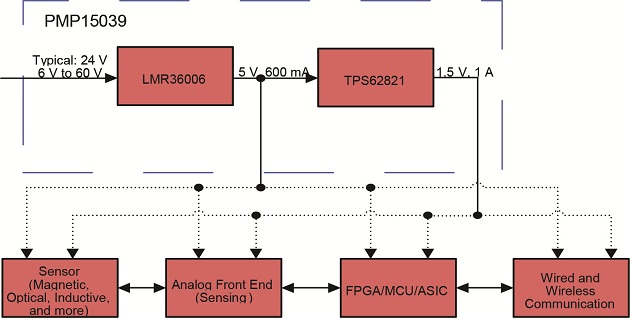
A standard field transmitter uses a nonisolated, wide VIN DC/DC converter as the primary power stage, paired with a point-of-load DC/DC converter. These two power rails are necessary to power the digital processing component of the system. Figure 1 shows the PMP15039 standard placement within the field transmitter system.
An AC drive feedback system converts SIN/COS differential inputs from the resolver or encoder into digital outputs to enable accurate rotor position feedback of the AC drives. The AC drive position feedback uses a nonisolated, wide VIN DC/DC converter as the primary power stage, paired with a point-of-load DC/DC converter. These two power rails are necessary for powering
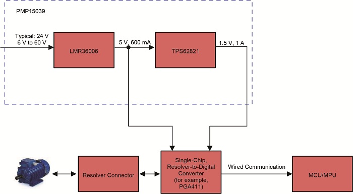
the digital processing component of the system. Figure 2 shows the PMP15039 standard placement within the AC drive position feedback system.
Key System Specifications
Table 1. Key System Specifications
| PARAMETER | SPECIFICATION |
| VIN minimum | 6 V |
| VIN maximum | 60 V |
| VIN nominal | 24 V |
| VOUT1 | 5 V |
| IOUT1 | 600 mA |
| VOUT2 | 1.5 V |
| IOUT2 | 1 A |
| U1 Feedback Voltage Accuracy | ±1.5 % |
| U2 Feedback Voltage Accuracy | 1 % |
| FSW_U1 | 1 MHz |
| FSW_U2 | 2.2 MHz |
| X – Dimension | 9.25 mm |
| Y – Dimension | 18 mm |
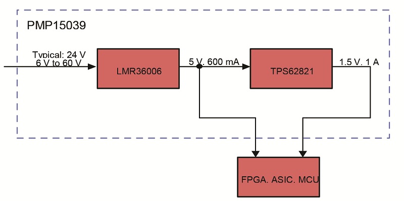
Block Diagram
Figure 3 shows the PMP15039 block diagram.
- 1% Feedback Voltage Accuracy (Over Full Temperature Range)
- Adjustable 0.6-V to 4-V output
- Maximum current load: 1 A for TPS62821, 2 A for TPS62822, and 3 A for TPS62823
- QFN package: 1.5 mm × 2 mm
System Design Theory
The PMP15039 reference design is the power management subsystem for industrial sensor applications that require dual outputs to power the digital processor. The reference design uses a wide VIN converter (LMR36006) and a point-of-load converter (TPS62821) in a two-stage power supply with an optimized switching frequency, temperature range, and form factor. The PMP15039 was designed specifically for field transmitters and AC drive position feedback applications, but the LMR360xx and TPS282x families of devices offer the flexibility to use this size-optimized layout for the various power demands of additional industrial applications.
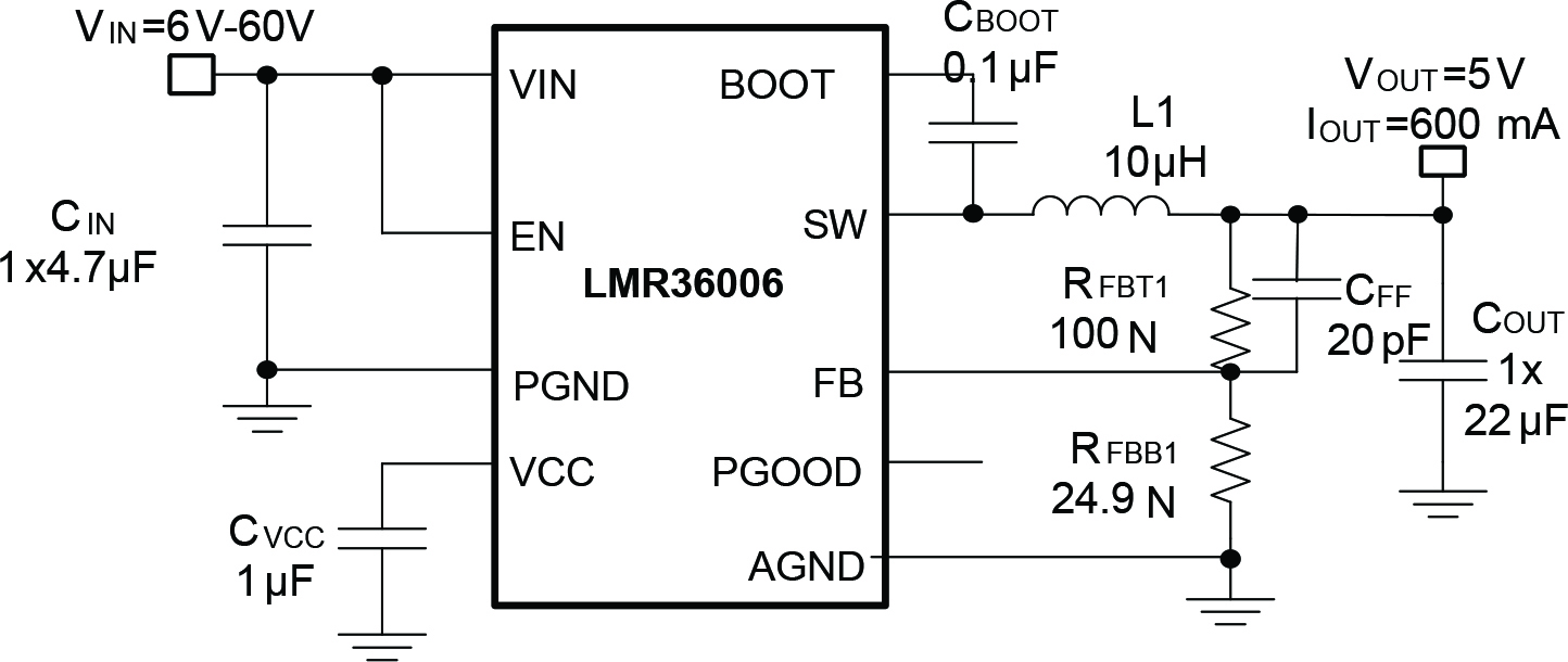
The LMR36006 synchronous buck converter is a wide input voltage, low quiescent current, highperformance regulator with internal compensation. The LMR36006 was chosen as the front-end, wide VIN converter for the PMP15039 because of the small package size (3 mm × 2 mm), the switching frequency, the 600-mA current capability, and the input voltage range of the regulator. The operating frequency for the LMR36006 regulator is 1 MHz, and the device implements a precise current limit. Consequently, the output filter size and component values are minimized. The device is designed with a flip-chip or HotRod technology, which greatly reduces the parasitic inductance of the pins. In addition, the layout of the device can help reduce the radiated noise generated by switching action through the partial cancellation of the current-generated magnetic field. Figure 4 shows the schematic of the front-end DC/DC converter.
For the PMP15039, the LMR36006 output voltage is set to 5 V with a resistor divider from FB to VOUT. The top feedback resistor (RFBT) is set to 100 kΩ, and Equation 1 calculates the bottom resistor (RFBB).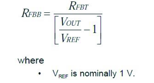 For this 5-V example, values are RFBT = 100 kΩ and RFBB = 24.9 kΩ. Depending on the power requirement of the downstream digital component, the output voltage can be adjusted.
To scale the output voltage for specific system requirements, the output feedback resistors can be resized. For example, if a MCU requires a typical power rail of 3.3 V, the output voltage can be adapted by recalculating RFBB. For this 3.3-V example, values would be RFBT = 100 kΩ and RFBB = 43.5 kΩ. Furthermore, the PMP15039 output filter (L1 and COUT) will support the output voltage adjustment.
When scaling the output voltage from 5 V to 3.3 V, the corresponding output power capability of the LMR36006 will decrease from 3 W to 2 W. To increase the power capability of the PMP15039 up to 7.5 W at 5 VOUT and 5 W at 3.3 VOUT, the pin-compatible LMR36015 offers a maximum output load current of 1.5 A. To adapt the design to the LMR36015, the output filter (L1 and COUT) must be modified appropriately. TI recommends that the user modify the L1 to 4.7 µH and the COUT to 33 µF. Also, the saturation current of the inductor must support the increased current capability and peak current limit of 3 A. Powered iron cores exhibit a soft saturation current, which allows some relaxation in the current rating of the inductor.
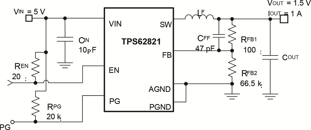
The TPS62821 synchronous buck converter is a low quiescent current, high-performance point-of-load converter. The TPS62821 converter was chosen for the PMP15039 because of the small package size of the TPS62821 (2 mm × 1.5 mm), the 2.2-MHz switching frequency, the 1-A current capability, the high efficiency, and the feedback voltage accuracy of 1%. Both the LMR36006 and TPS62821 devices belong to a family of devices that offer various output power capabilities. With an operating frequency of 2.2 MHz, and a 2-mm × 1.5-mm QFN package, the TPS62821 device enables a small solution size. Based on the DCS-Control topology, PMP15039 provides a fast transient response. Figure 5 shows the schematic of the point-of-load DC/DC converter.
For the PMP15039, the TPS62821 stage is set to 1.5 V with feedback resistors from FB to VOUT. The top feedback resistor (RFBT) is set to 100 kΩ, and Equation 1 calculates the bottom resistor (RFBB). VREF is nominally 600 mV. For this 1.5-V example, values are RFBT = 100 kΩ and RFBB = 66.5 kΩ.
Depending on the power requirement of the downstream controller, the TPS62821 output voltage can be adjusted. For example, for controllers that require a typical power rail of 2.5-V, the output voltage can be adapted by recalculating RFBT and RFBB. For this 2.5-V example, the values would be RFBT = 475 kΩ and RFBB = 150 kΩ. See Table 2 for the recommended feedback resistor values for typical output voltages.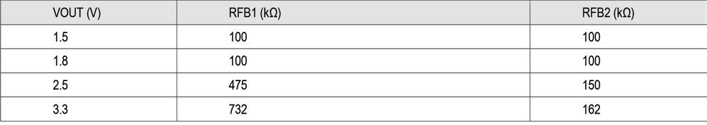
Table 2. Feedback Resistor Values for Typical Output Voltages
Furthermore, in addition to the described changes for the front-end converter to modify the output power capability, the point-of-load converter may also need to support a higher load current. To adapt the TPS62821 to system-specific power requirements, the pin-compatible TPS62822 supplies a maximum load current of 2 A and TPS62823 supplies a maximum load current of 3 A. To modify the output filter accordingly, the saturation current of the inductor must support the increased current capability.
Hardware
The following steps outline the hardware setup.
Connect a DC power supply to the board input as shown in Figure 6.
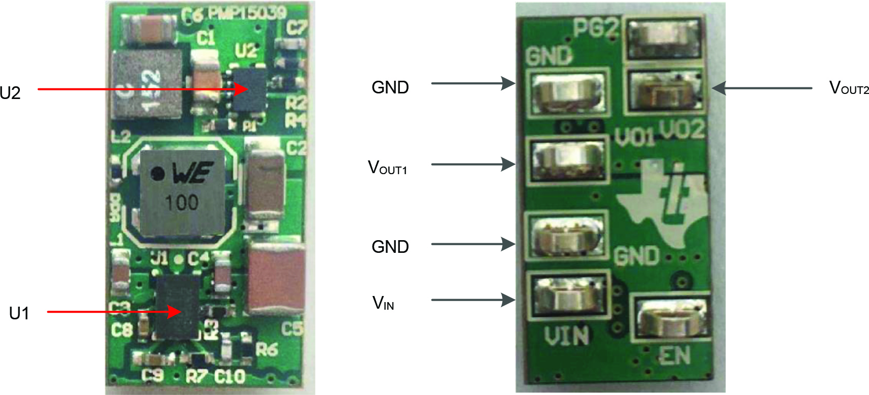
Connect an electronic or resistive load to the dual outputs (VOUT1 and VOUT2) to imitate the typical load as shown in Figure 6.
Thermal Data
The infrared (IR) thermal image in Figure 7 was taken at steady-state with VIN = 24 V and the TPS62821 output at a full load of 1 A (no airflow). The ambient temperature is approximately 22°C. The maximum IC temperature is 47°C.
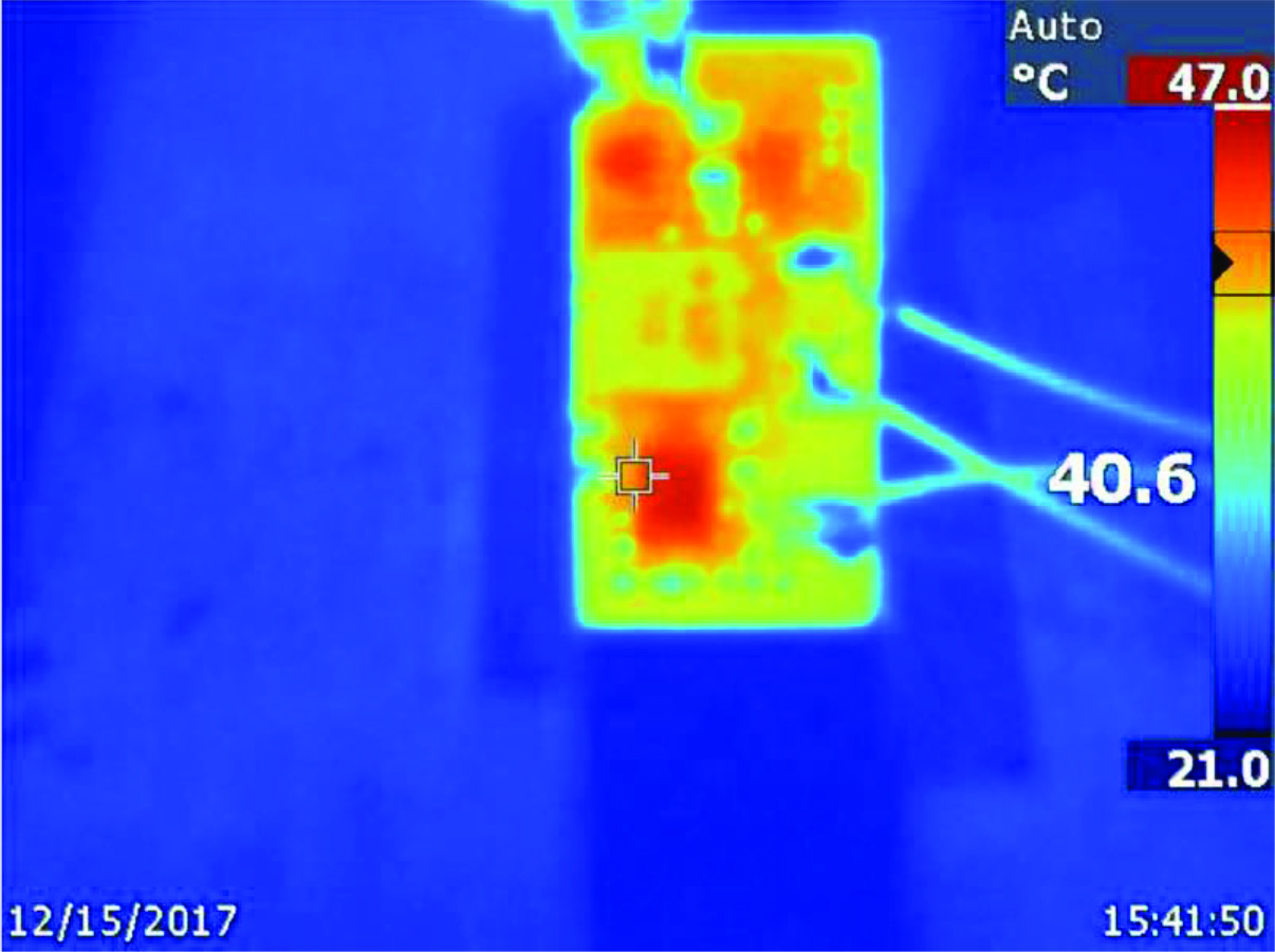
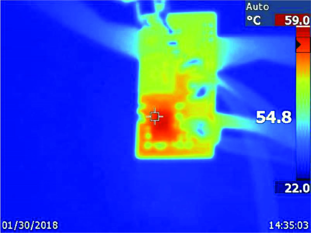
Figure 8 was taken at steady-state with VIN = 24 V and the LMR36006 output at a load of 300 mA ( no airflow) and TPS62821 output at a load of 1 A (no airflow). The ambient temperature is approximately 22°C. The maximum IC temperature is 59°C.
Efficiency Data
Figures 9 and Figure 10 show the efficiency of the PMP15039 device versus a load current of U2, TPS62821.
Output Current (A) D005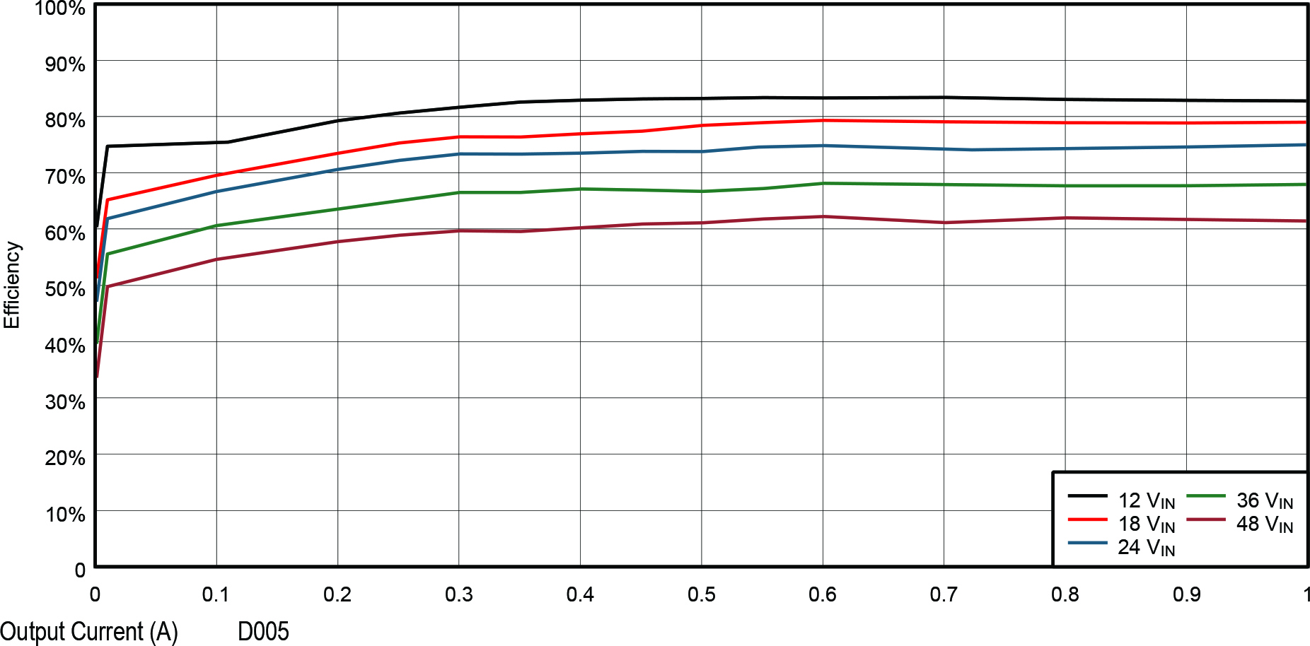
Figure 9. System Efficiency Versus Load Current: IOUT1 = 0 A, IOUT2= 0 A to 1 A
Output Current (A) D001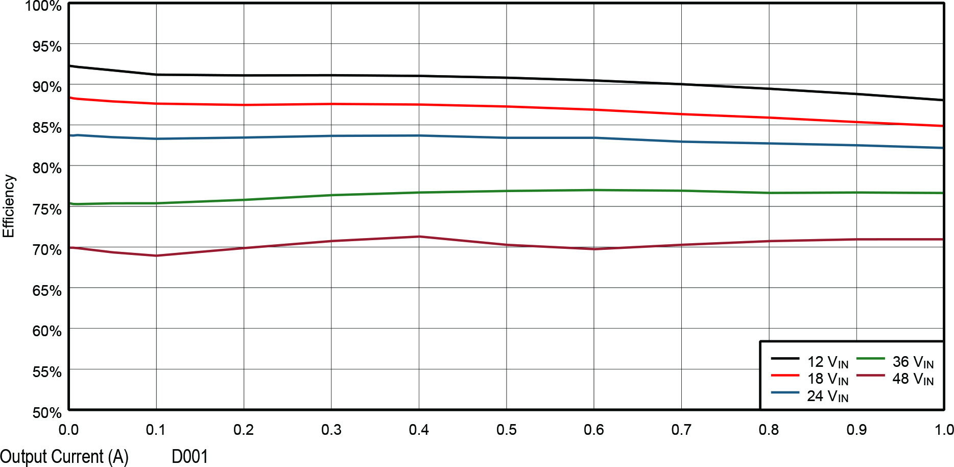
Figure 10. System Efficiency Versus Load Current: IOUT1 = 0.3 A, IOUT2 = 0 A to 1 A
Output Load Regulation
Figures 11 and Figure 12 show the output load regulation of the converter.
Output Current (A) D003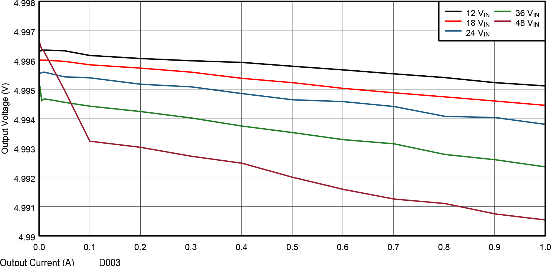
Figure 11. LMR36006 Load Regulation: VOUT1 vs IOUT2
Output Current (A) D002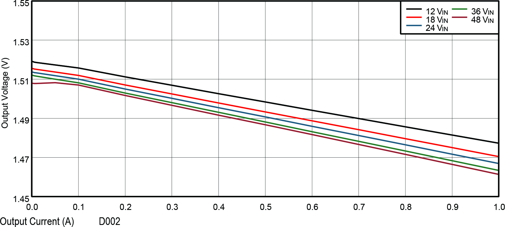
Figure 12. TPS62821 Load Regulation: VOUT2 vs IOUT2
Start-Up Waveforms
Figure 13 shows the start-up waveform at a 24-V input and no load. Figure 14 shows the start-up waveform at the 24-V input and 1-A load at VOUT2.