


Researchers at the University of Texas at Dallas have designed the fully actuated probe stage of an atomic force microscope (AFM) on a single chip with the help of a readily available silicon-on-insulator MEMS manufacturing process.
Additional driving circuitry, an external signal conditioning board and a few stepper motors (to approach the samples) are all what would be needed to build a fully functional AFM possibly orders of magnitude simpler and cheaper than today’s bulkier solutions.


In their paper, “On-Chip Dynamic Mode Atomic Force Microscopy: A Silicon-on-Insulator MEMS Approach,” published in the Journal of Microelectromechanical Systems, the researchers detailed the fabrication and characterisation of such a MEMS-based AFM probe-scanner.
The main novelty is that rather than relying on the deflection of a laser beam on the back of a micro-cantilever to monitor the AFM’s tip position, here the MEMS probe-stage integrates not only X-Y electrostatic actuators for scanning a sample but also a piezoelectric layer able to both actuate the micro-cantilever out-of-plane and senses its deflection. Thanks to this integrated piezoelectric feedback loop, the intricate three-degree-of-freedom design can be operated in tapping-mode, yielding topographic AFM images with an imaging range of up to 8μm × 8μm.
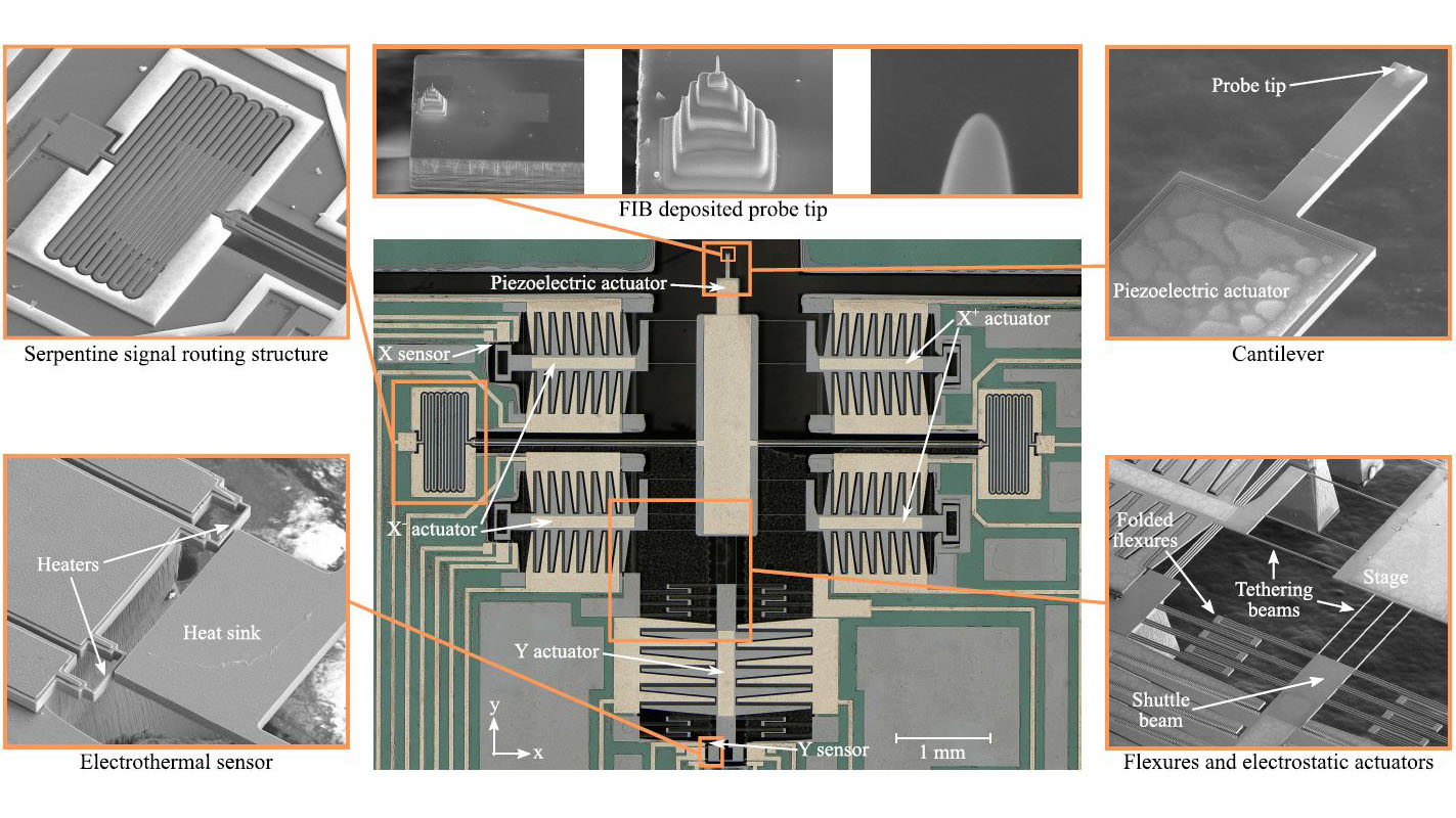
In previous research, the authors had devised the first subsystem of an AFM, an in-plane MEMS nano-positioner with electrostatic comb-finger actuators and electrothermal sensors. They now improved their design with out-of-plane actuation (third dimension) by depositing a thin piezoelectric AlN layer on the back of the probe’s supporting micro-cantilever. “Piezoelectric transduction,” they write, “seems to be the only one capable of simultaneously serving as an actuator and a sensor even with a single active layer.”
The entire MEMS structure with its three degrees of freedom is only 10μm thick. In this experiment, a sharp probe platinum tip (1.5μm long and about 40nm in diameter) was added to the MEMS using ion beam deposition, but in the future, the authors will try to incorporate the tip fabrication step into the MEMS device fabrication.