STMicroelectronics is a global semiconductor leader delivering intelligent and energy-efficient products and solutions that power electronics at the heart of everyday life. ST is enabling smarter driving and smarter factories, cities and homes, along with the next generation of mobile and Internet of Things devices.
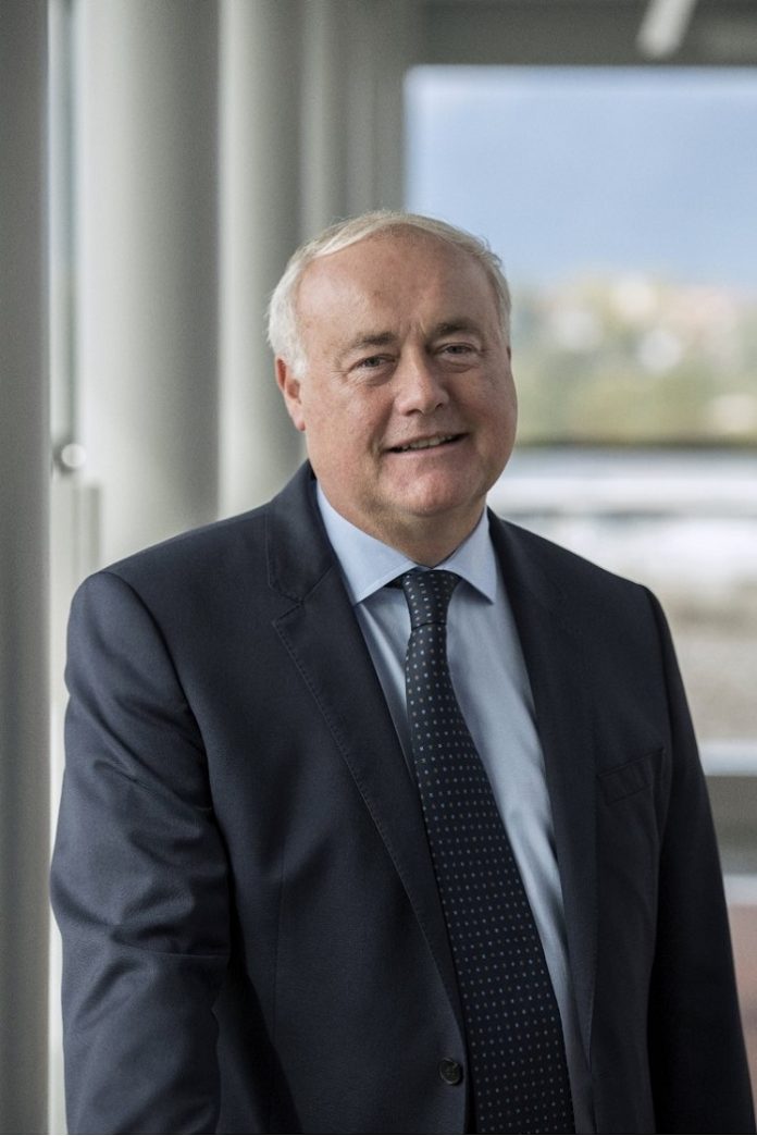
During the Virtual Media Event, Jean-Marc highlighted on the following:
- Long-term investments in the key technologies needed to support the enabling trends.
- Targeting specific markets and applications that benefit from ST’s technologies and drive the adoption.
- Creating innovative, sustainable technologies in a sustainable way.
- Developing products and solutions that meet the needs of ST’s customers.
- Well-positioned to grow in the region and earn an increasing share of the market.
ST addresses four end markets viz. automotive, industrial, personal electronics, communications equipment and computers and peripherals. STMicroelectronics strategy stems from key long-term enablers like Smart Mobility, Power & Energy and Internet of Things and 5G:
Smart Mobility: ST provides innovative solutions to driving safer, greener and more connected for everyone. The solutions increase safety for road users and driver comfort and convenience.
Power & Energy: It increases energy efficiency everywhere and supports the use of renewable energy sources.
Internet of things & 5G: ST also provides sensors, embedded processing solutions, connectivity, security and power management, as well as tools and ecosystems to make development fast and easy.
Investments: ST plans massive investments of $1.5 Billion in Research & Development per year. The company plans to invest $2.0 Billion in CAPEX in 2021 to support the strong market demand and strategic initiatives. ST also plans to target acquisitions to accelerate technology and portfolio development.
Carbon Neutrality: ST is committed to achieve Carbon Neutrality by 2027, Compliance with the 1.5°C scenario (Paris COP21) by 2025 and sourcing 100% renewable energy by 2027.
On asking what will be the new technology trends that will dominate the semiconductor industry in 2021? What will be ST’s key focus in the current year in COVID-19 period, Jean-Marc commented at length, “You have to break down the semiconductor landscape into 3 important categories. The first one is the world of standalone electronics, computers and communication. The base technology is CMOS FinFET. Today, the state of art production is 5 nanometers with some variants using FinFET architecture. This is a massive introduction of extreme UV photolithography to replace progressively the multiple patterning way of processing devices. We know that now main players like Samsung, TSMC and Intel in cooperation with IBM, they are developing next-generation, 3/2 nanometer, where you will have some kind of disruption, as they will move most likely to nanosheet, gate-all-around the technology in order to continue Moore’s law. If they are successful in setting up the new architecture, we can expect Moore’s law to continue for a certain number of years”.
“Also, what is important to understand and address this kind of business, you will also need to have some way to make better integration. It is called 3D heterogeneous. It refers to the capability of stacking many dies vertically to have the smallest system on a chip, system in a module and system in a package”.
He further stated, “As for the memory and non-flash, or DRAM, they also follow a similar process in terms of storage capability and energy consumption as they are becoming more and more energy-efficient and have better and better performance”.
“Now I move to a world where we are more exposed to diversified semiconductor companies, here there is a core for all the technologies which are used in this world. There are companies like TI, NXP, Infineon, Renesas and ST. It is wide. First, you have the block of the mature 8 inch from 0.5 micron to 110 nanometers. Then you have the block of the mature 12 inch, so from 19 nanometer to 28 nanometer. For 28 nanometers, we see it as an innovation for the transistor gate. So this is the block for the mature 12 inch”.
“Then you enter the world of the most advanced 12 inch, with the FinFET area. Of course, this world of diversified products is starting to design and manufacture soon the 16 nanometer FinFET for embedded processing solution and power processing solution to address automotive and some specific industries”.
“Maybe we go to another node between 10 nanometer and 12-nanometer FD-SOI. This diversified world is very spread from 0.5 micron to 110 nanometers, 8 inch, and then from 19 nanometer to 28-nanometer, and to 12 inch mature, and then starting to go into the FinFET double patterning, triple patterning zone. This is what I am seeing”.
“Then in parallel for the diversified world, there is strong innovation in material for the power and SiC (innovation in assembly, innovation in wafer processors, innovation in the raw material to convert into the 8 inch, and innovation in the new capability to optimize the number of wafers from an ingot). So in power, you have strong innovation as well”.
Jean-Marc concluded, “For optical sensing solutions, it is the same, as you want optical sensing solutions to have more performance, smaller footprint on the devices, affordability in terms of cost, and ST is pushing this innovation. MEMS is very similar. More accuracy, and less power consumption. So there is no unique response from the diversified world. Because there is a mix between the CMOS-based (analog, mixed signals, radiofrequency, embedded flash) world of power, sensors, and pure analog. So here not only you have the memory, the world of computation and communication. Also in the diversified world, 3D integration, we also offer the capability of great innovation. So for 2021, I repeat that the success of the semiconductor lies in the capability to innovate. For the customers, please do not limit your innovations, semiconductors will always answer your needs. It is based on efforts of the global industry, with important players of the right scale investing the right amount in R&D, innovation and design in order to achieve the best innovation in the world with affordable cost”.
ST’s outlook and strategy for car electrification and digitalization and improvements made to SiC devices:
On the improvement of SiC devices Jean-Marc stated, “For assembly MOSFET on SiC are available either in custom-designed modules or through more application-specific standard modules”.
“The first area of improvement is the performance improvement of modules. The mission profile of electric cars, specifically the two main applications with SiC, is the improvement of the inverter, onboard charger, and DC/DC converter”.
“For process, we are introducing in mass production of our Generation 3 which is based on planar technology. We are already developing Generation 4. ST continuously improves the performance of MOSFET in the area of high tension and pure electrical performance.
Global supply chains during pandemic and its impact on the automotive industry:
Replying to global supply chains Jean-Marc stated, “There is a gap between the demand the semiconductor industry is facing since December last year, versus the manufacturing capacity the semiconductor industry has prepared and invested for 2021”.
“ST, assuming the demand a few months ago, prepared to bill revenue of around $11 billion. But the demand now is above $15 billion. The industry has prepared itself to bill $9500 billion revenue, while the demand was basically 30~35% above this capacity. So it is not the question of shortage. It is a question that everybody across the value chain from electronics, OEM, EMS, customers both from standalone electronics and embedded electronics did not prepare properly for this boom”.
“For meet the demand in the short time we moved our CAPEX from $1.5 billion to $2 billion as announced in December. We reacted immediately to increase the capacity to support the market. However, the gap is still 25%. For the medium term for 2022 and 2023 we are discussing with our customers”.
Independence in semiconductor supply chain through creating local production facilities to ease dependence on foreign countries for continuous supply:
Jean-Marc stated, “It is something critical. Today when you look at the competitive landscape of the semiconductor industry, I repeat the diversified blocks including computation, communication, memory, and storage. There are basically 25 companies with a market cap above 10 billion dollars. You have two kinds of operating models. One is fabless and the other one is IDM. In the foundry landscape, 3 companies listed with a market CAP of more than 10 billion dollars, and they are TSMC, UMC and SMIC. Then you have non-listed sites like GlobalFoundries and Samsung. What is important at this stage is that the semiconductor industry continues to grow and innovate. Countries provide incentives to attract and encourage innovation and manufacturing in a fair and balanced way. This is what we expect and plan”.
“We are not planning in a world where you can do business only if you develop IP locally, design locally, do R&D locally and manufacture locally. This is not the world we plan. We see important political willingness through incentive programs which I expect to drive fair competition, allowing the industry to progress. I think it is normal with various shortages at this time”.
“Also some customers are also changing their minds. Customers are also open to capital participation and CAPEX participation. So we see this trend as something new, but we do not plan for the total silos of countries in the world where everyone becomes independent. Because do not forget that behind a wafer fab and technology, you have the OSAT, a complex assembly and packaging process. Then you have the equipment maker, wafer assembly and then EDA to provide IPs and design tools and also R&D is very important. Artificial intelligence is coming, then you also have the process material maker. To make silos like America, Europe, China, Taiwan, South Korea and Japan, the answer is No. This will not happen”.
“Yes, we see change in the manufacturing landscape with less concentration but this is not something that makes us feel afraid. We will definitely adapt ourselves and I repeat that our strategy stems from the megatrend of society. Our operation model is the IDM. We have important infrastructure in Europe and Asia. We are spreading our design capabilities and application labs everywhere in the world. So we remain a global company, with diversified semiconductors, focusing on automotive and industrial. We will take into account the shift of the landscape. But we do not plan for the catastrophic decoupled world”.
For more information, visit www.st.com


