STMicro’s manufacturing strategy is a study on a long-range plan to use the resources of the manufacturing system to support the business strategy and in turn meet the business objectives.
STMicroelectronics is an independent integrated device manufacturer with in-house manufacturing complemented by outsourcing partners. ST’s manufacturing strategy is a key enabler for future growth and in the last two years the company has accelerated capacity investments to cope with the unprecedented semiconductor demand growth.
ST’s manufacturing footprint is being transformed with strategic investments in 300mm wafer manufacturing and growing wide bandgap technologies, with SiC and GaN migration to 200mm. The vertical integration of SiC will increase company’s value creation, to improved manufacturing efficiencies.
The company already has a unique position in 300mm as a high-volume manufacturer with digital technologies, including embedded non-volatile memory ranging from 90nm down to 28nm serving the bulk of technology requested by the industrial and automotive market. This makes ST’s manufacturing footprint unique among the peers.
Assembly testing, technology and manufacturing are also instrumental to ST competitiveness and customer service capabilities. ST develops manufacturing in-house, a huge variety of packages and complement internal production and technology offer with selected collaboration with subcontractors.
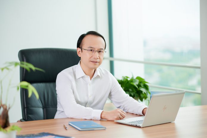
During a press meet Henry Cao, Executive Vice President, Sales and Marketing, China Region, STMicroelectronics gives an overview of ST’s manufacturing strategy. The excerpts of the interview are given below:
Introduction to Semiconductor Manufacturing:
Chip manufacturing is the process of creating individual packaged and tested integrated circuits (IC) from a semiconductor wafer. Semiconductor manufacturing process is quite complicated. Some of the mind-boggling facts are really astonishing to a lay man given below:
It requires 7 seconds to renew all the air in a fab cleanroom – typically bigger than a football stadium. It requires 1,000 times fewer airborne particles in a fab cleanroom than in a hospital operating room. The advanced transistors are 10,000 times smaller than the width of a human hair. By leveraging one ton of sand, we can make almost 5,000 pieces of 8-inch wafer. 40 km Distance covered by a wafer in the fab during processing. There are more than 100,000,000 transistors per square mm in the most advanced chips and more than 1,000,000,000,000 semiconductor chips made worldwide per year.
Exploring the limits: Semiconductor size – or node size – is indicated in nanometer, a unit that equals one billionth of a meter (or 0.000000001m). Semiconductor chips in terms of size are even smaller than the cat flea, human hair or even a virus. Chips with 14 and 10 nanometers are currently in mass production, but the industry continues to aim for smaller node sizes i.e. ten nanometers, seven, five and even three nanometers.
Semiconductor manufacturing cycle times
The manufacturing cycle time involves hundreds of steps and can take up to four months from design to mass production. Time is required to make a wafer involves electrical wafer sorting, assembly & testing, quality control and testing. Normally it takes 20 to even thirty 30 weeks. That is why ST asks its customers to plan their semiconductor requirements well in advance as to how many chips and what kind of chips they need.
Overview of manufacturing at ST: ST is an integrated device manufacturer. ST covers all the value chain, ranging from design, wafer fabrication to assembly, test, sales and support. ST covers fabless, foundry and back end (packaging & testing).
ST has a lot of manufacturing facilities across the world. For front end foundry the major locations are Sweden, France, Italy and Singapore. Packaging and testing facilities are in Italy, France, Morocco, Malta, Malaysia, Shenzhen and Philippines. ST has factories covering the front end and back end across many countries.
ST people strength: ST has a global presence. It has around 50,000 employees spread across the world. ST offers its customers multiple sources and integrated supply chain control. ST has different manufacturing locations – focusing on different technologies and products. ST has the capability to shift the production workload across different locations not to be impacted by a single location for whatever reason.
ST’s technologies enable product differentiation and customer success
ST has a rich portfolio of technologies, and most of the technologies are proprietary ones. For example, ST has smart power technologies covering BCD, STi²GaN and VIPower. In power technologies ST has Power MOSFET, IGBT, SiC, GaN. Under MEMS technologies ST has analog mixed-signal technologies. Under digital technology ST has FD-SOI. Under flash technology ST has a lot of special technologies focusing on embedded flash, CMOS technology, RF CMOS and BiCMOS. For packaging technologies ST is quite nimble and resilient in providing the best combinations of lead frame, laminate, sensor module, wafer level, and all kinds of technologies.
ST’s technology R&D is integrated with fabs: ST’s factory has technology R&D integrated into it. The company has facilities for design close to the manufacturing unit. Factory/fab has human resources focusing on R&D and design to provide continuous innovation of the technologies.
ST also focuses on the innovations in assembly and testing. ST is also working with OSAT, the subcontractors for packaging and testing to continuously innovate with the latest technology to serve end markets such as smart mobility, power & energy, and IoT and connectivity market.
ST manufacturing strategy:
ST’s technology R&D and manufacturing strategy is the key enablers of business: ST is investing in competitive proprietary technologies and in-house manufacturing complemented by outsourcing, creating a reliable supply chain for its customers. ST has plans to double the internal manufacturing capacity for the 300 millimeter, from 2022 to 2025.
ST is Focusing on investing in Silicon Carbide, and GaN and building internal technology capacity to offer 200 millimeter, and plan to achieve the internal production of the 8 inch in 2023. ST is working with outsourcing partners to have Support from foundries & OSATs on capacity growth, leading-edge digital technologies, and packages.
Strategic manufacturing programs: For 300 mm capacity expansion ST has manufacturing units at Crolles, France, and Agrate, Italy to double the capacity by 2025. For Wide bandgap capacity expansion ST has Catania unit on SiC technologies and Tours unit, France on GaN.
ST partners with GlobalFoundries for Sustainable manufacturing: ST and GlobalFoundries have set up a new manufacturing facility in France. It is ISO certified for environmental and energy management, focusing on FD-SOI technologies. It is the world’s cleanest fab in the semiconductor industry.
Integrated SiC substrate manufacturing facility: ST has planned to integrate the SiC substrate into the entire manufacturing strategy for SiC devices and technologies. ST acquired Norstel in 2019 to expand the capacity, including moving production from Norrköping in Sweden to Catania in Italy. It will be a first of a kind in Europe for the production in volume of 150 millimeter SiC epitaxial substrate which is 6 inch epi, integrating all steps in the production flow, and this is the site to develop the 8 inch wafer in the near future. The production is expected to start in 2023.
Catania is an important site for ST power innovation: ST is leading in SiC R&D with a large portfolio of key patents. It is the home to the largest SiC R&D and manufacturing operations. It has an established eco-system on power electronics with long-term, successful collaboration between ST and different stakeholders.
ST will increase from 17% of our total production mix with 12 inch capacity to 33% in 2025. And the main sites for 12 inch are Crolles in France and Agrate in Italy.
For Agrate 300 mm fab, it’s progressing smoothly to ramp up in 2023. Most of the production qualification has been planned to be completed by the first half of this year. Fast ramp thanks to capacity sharing with Tower Semiconductor. The first wafer production lot has been successfully released in October, 2022.
ST is accelerating the expansion of SiC device manufacturing capacity. More than 100 million devices shipped to automotive customers. For capacity, ST has expanded it more than 2.5 X by the year 2022. Catania and Singapore are the main sites for SiC manufacturing and for assembly and testing of SiC Shenzhen and Bouskoura are the sites.
ST has acquired Norstel hence plans to have more than 40% internal supply of substrate by 2024.
ST is focusing a lot on GaN technology because it’s a huge complementary technology to SiC to cover the customer demand for power devices. ST has power conversion GaN and the RF-power GaN, and has 200 mm power GaNfab in Tours with fab qualification in 2022. ST has 6 inch RF-GaN in Catania and has fab qualification available in 2022.
Strategic manufacturing outsourcing: ST is working with outsourcing partners for strategic manufacturing. For Front end, ST is leveraging 80% from internal source for fab capacity and working with partners for 20% of external source. For Back end, ST provides 65% of the internal capacity while sourcing from partners OSAT provides 35% of the capacity.
ST’s Manufacturing sites:
Agrate: The Agrate Brianza is one of ST’s main front-end fabs as well as R&D center for Smart Power and MEMS technologies. The site also carries out EWS activities. In addition to the long-running 200 mm fab, ST is building out a state-of-the-art 300 mm fab which will be qualified for production in the first half of 2023. Main technologies: BCD including Advanced BCD with PCM and galvanic isolation MEMS sensors & actuator (ThELMA, PƐTRA, TMOS).
Bouskoura: Bouskoura represents one of the most advanced chip packing and testing facilities in the world. It supplies products to industries with the highest quality requirements such as automotive. Main technologies: SO, TSSOP, PSO, PSSO, STPAK, Module & Micromodules
Calamba: Calamba plant is a sophisticated IC and module back-end manufacturing facility, which assembles and tests a diverse range of products. These include power devices, RF, memories, touch-screen controllers, microcontrollers, MEMS, and optical sensors. The site plays an important role in advancing new packaging technologies, such as ultra-thin wafer, multi-stack and multi-IO assembly and higher-value module solutions. Main technologies: QFN, QFN-MR, BGA, LGA, WLCSP, Micromodules, Optical Modules
Catania: Catania hosts front-end manufacturing, Electrical Wafer Sort (EWS), R&D, labs, and product design. It manufactures products in Silicon, SiCand GaN, addressing power and smart power applications for automotive, industrial & communications markets. It also produces analog ICs and ASSP for a broad range of applications. Main technologies: Silicon Carbide (SiC), Gallium Nitride (GaN), Power transistors, Smart Power (BCD, VIPower).
Crolles: Crolles houses design, R&D and production activities for the development and manufacturing of ICs in digital technologies on 200 mm and 300 mm silicon wafers. This includes microcontrollers, image sensors, and other advanced devices based on differentiated CMOS technologies. Main technologies: FD-SOI, CMOS, BICMOS
Kirkop: Kirkop plant is the largest back-end site in Europe. It is a world-class assembly and testing plant for a wide range of products serving automotive and personal electronics customers. Main technologies: MEMS sensors, QFP, BGA and LGA
Marcianise: Marcianise site supports the deployment of secure microcontrollers. The site has fully featured smartcard manufacturing lines, and the capability to personalize secure ICs through dedicated SW development and services. Main technologies: Smartcards, Secure software and personalization services
Muar: Muar is an advanced back-end manufacturing facility specializing in high-complexity and high-reliability packages. A major portion of the production volume is dedicated to automotive products and the site is a leader in automotive product engineering and test development. Main technologies: QFP –PSSO /PSO, PQFN, BGA , HiQuad, SOIC
Norrköpping: Norrköpping is a center of excellence for Silicon Carbide (SiC) substrate technology and manufacturing. It is the pilot line for the manufacturing of conductive and semi-insulating SiC substrates and epitaxial layers. Main technologies: Silicon Carbide
Rennes: ST serves the complete needs of space and aerospace customers for plastic rad-hardened devices and for ceramic and metallic hermetic packages. Main technologies: Analog, Logic, Schottky Diodes & Rectifiers, Interfaces, Power management, Bipolar & MOSFET transistors.
Rousset: Rousset is a fully integrated facility that includes manufacturing, electrical testing, R&D, new product design, and marketing activities. The site includes a 200 mm wafer manufacturing plant for standard and secure microcontrollers, and application-specific products, and an electrical test center for 200 mm and 300 mm wafers from various ST manufacturing plants and subcontractors. Main technologies: Embedded flash, EEPROM, CMOS, BiCMOS, images, and analog/RF.
Shenzhen: Shenzhen plant packages and tests a broad range of semiconductor components including power transistors, advanced SiC power modules, application-specific ICs, memory, MCUs, standard linear, VIPowerdevices, wafer level packages, and optical modules. Main technologies: STPAK, Power Plastic, Proximity sensor, WLCSP, SO / TSSOP, SSDIP
Singapore: Singapore is one of our largest front-end manufacturing facilities serving a broad range of applications. They also house the largest electrical wafer sorting (EWS) operations as well as packaging research and development activities. This new R&D line looks to advance Piezoelectric MEMS technologies to boost innovation and accelerate development of new materials. Main technologies: Mesa Glass, Planar, RF filters, Power GaN
Tours: Tours designs and manufactures components on silicon and glass substrates, such as protection diodes, rectifiers, thyristors, Triacsand filters, targeting a wide variety of electronic applications. Main technologies: Mesa glass, planar, RF filters, and power GaN.
Sustainability in manufacturing
ST is focusing on sustainability to reach carbon neutrality by 2027 on the company level. ST creates technology for a sustainable world by prioritizing people thus protecting the planet thus generating long-term value for all stakeholders. ST has achieved quite a lot of results in terms of water consumption, electricity consumption and water recycled rate.
ST’s EHS team focusing on manufacturing sites energy management from health safety. All the sites worked on 53 energy management improvement projects, saving 35 GWh of energies.
ST is trying to reduce carbon footprint in Singapore. ST adopted a district cooling system at ST’s single largest wafer-fabrication site by volume globally. It eliminated up to 120,000 tons of carbon from the environment, which is equivalent to 30% of ST Singapore’s carbon emissions in 2021.
Water Management: Manufacturing sites produce ultra-clean water and continuously improve wastewater treatments and water discharge quality in order to reduce carbon footprint of all these sites.
ST focuses on zero waste and recycling. ST targets to work with customers and partners to strive for zero waste while promoting a circular economy.
ST is investing in the areas of digital transformation and Industry 4.0.
ST is leveraging digital technologies to reduce waste, to strengthen supply chain and product life cycle management. ST connects and digitalizes products related to information and processes for a more efficient and effective innovation engine. It leverages the digital technologies to analyze manufacturing data, to industrialize ST’s manufacturing data and analytics capabilities.
ST has a highly automated fab. For example, transporting materials is 100% automated, production 100% automated, automated processes 95% of the dispatching is automated. ST’s fabs can run 24 hours, 365 days a year.
ST is digitalizing the semiconductor factory floor: Industrializing manufacturing data & analytics capabilities, contributing to improving manufacturing quality, yield, equipment productivity, and manufacturing cost.
ST uses the latest Industry 4.0 Technologies such as mixed reality for remote maintenance autonomous intelligent vehicles to enhance the automation of the entire factory. ST is leveraging digital twins technologies, especially for the 300 mm fabs at Crolles and Agrate.
The Importance of Embracing Technology in Manufacturing
In response to a question with ELE Times as ‘What is the importance of embracing technology in manufacturing for ST? How has the use of technology changed over the years for semiconductor players, Henry Cao replied, “Technology is evolving at an astonishing pace, changing the way we live and the way we do business. Today, companies big and small, across all industries, need to prioritize technology in order to effectively compete, keep operations running efficiently, and deliver greater value to customers.
Embracing technology, in the manufacturing industry, is important for several reasons. It improves efficiency and productivity, resulting in lower production costs and increased profitability. Today, semiconductor players rely heavily on advanced manufacturing technologies such as lithography, chemical vapor deposition, and plasma etching to create ever-smaller and more complex devices.
Advancements in technology are enabling manufacturers to streamline production processes, innovate at a faster pace, reduce costs and deliver higher quality products to meet customer demand. Because of its versatility and ease of use, there are a number of areas within manufacturing where technology is being harnessed by ST. By investing in the technologies, we are able to save money and improve our value proposition to customers and potential customers, differentiating the unique products we offer in the market.
ST has been incorporating such technologies for years, mastering the semiconductor supply chain with state-of-the-art manufacturing facilities. We also use data analytics and artificial intelligence to monitor and optimize the production processes, ensuring that they are operating at peak efficiency and quality. Our technologies enable smarter mobility, more efficient power and energy management, and the wide-scale deployment of the Internet of Things and connectivity. IoT sensors can be used to monitor equipment and machines, collect data on their performance, and alert operators to any issues that arise. This technology is an example of what we at ST have embraced and are perfecting for manufacturing”.


