The design requirements for wearable devices are unique among embedded systems. Design engineers don’t have the freedom to trade size against weight, or performance for power. When it comes to wearables, smaller isn’t just better, it is essential.
As semiconductor processes evolve, they deliver smaller integrated devices with lower power dissipation. These are important contributors to expanding the potential applications for wearable technology. Engineers have greater design freedom with access to more capable integrated devices.


Today, most wearable products are worn on the wrist. Smartwatches are multifunctional but fitness bands that track activity are rising in popularity. Fitness and well-being are closely related to medicine and healthcare and in this context, the wrist is merely convenient. It provides a good place to monitor movement as well as pulse rate. Heart health can also be measured using electrocardiogram methodology, with the wrist providing one point of contact.
Transducers provide the interface between the physical and digital domains. Electronic (MEMS-based inertial measurement) and mechanical (Piezo) sensors are perhaps the best known. Other types of sensors exist and are being developed, particularly for wearable medical devices. Optical sensors use different wavelengths to penetrate the skin by a defined depth and analyze the reflections to gain insights into the health of the wearer. Similarly, near-field radio frequency sensors can detect breathing patterns and lung capacity. Microfluidic biosensors are used in wearable medical devices to detect markers in sweat.
Future wearable technology will be more aligned with our own senses. Smart earwear and eyewear leverage augmented and virtual reality and can be used in all types of vertical markets. Bodywear, including foot and hand, provide a more personalized experience by tracking the wearer’s movements with greater accuracy.
The incredible rise of the wearable
 Wearable devices vary in their application, but as a market sector, they share common features. They need to be as unobtrusive as possible, which means size and weight will drive design. The availability of physically small integrated devices is part of the solution but powering the device will be fundamental. While research is ongoing around self-powered wearable sensors, the majority will still need a battery.
New battery technologies for wearables
Battery capacity is also limited by size. The popular CR2032 coin cell battery measures 20 mm in diameter and 3.2 mm thick. It provides 220 mAh of power at 3 V. To get a week of use time out of wearable using a battery with a capacity of 220 mAh, the device will need to consume, on average, around 130 uA.
Using electric vehicles as a comparison, an electric car will return approximately 5 miles of range per kWh of power. EV batteries are reported to have an energy density of around 250 Wh/kg. A battery that can provide a range of 500 miles will weigh around 400 kg, while a 200-mile range battery would be around 160 kg. The same applies to anything battery-powered, including wearables. The larger the battery the longer the usable lifetime between battery charges or recharges, but the device will be larger, heavier, and possibly more expensive.
Solid-state lithium battery technology is being adopted by the EV market. It is reportedly safer than lithium-ion technology due to the solid electrolyte. This inherent safety means the battery casing can be thinner, reducing the overall weight and increasing the energy density. The same is true for wearables, in the form of solid-state micro batteries. Leaders in this field are reporting solid-state micro batteries with twice the energy density of conventional lithium-ion coin cell batteries.
As the industry moves toward body wearables, the shape of batteries becomes more flexible. This is the case for soft lithium-ion rechargeable batteries that can be manufactured in pliable pouches. The format supports larger batteries with a relatively lower weight for power density. These could be used in smart clothing, for example, by incorporating them into the fabric.
Ultra-low-power process technologies
The semiconductor industry is acutely aware of power. This doesn’t just relate to how much active power a device uses; it also impacts the amount of heat a device can dissipate as transistor density increases. There is a link between transistor scaling and energy density, so developing low-power processes is important to the future of semiconductor integration.
Several process technologies have emerged over time. These include a fully depleted silicon-on-insulator (FD-SOI), which adds an insulating layer to the bulk substrate to reduce body capacitance. This improves speed and lowers noise, which can be exploited to reduce the operating voltage and, by extension, power consumption. Its lower noise has also prompted some manufacturers to use it for analog ICs.
Another innovative technology involves operating the transistors at a voltage lower than the conventional threshold used. This so-called subthreshold approach for digital ICs delivers power savings due to the same principal; lower operating voltage equals lower power.
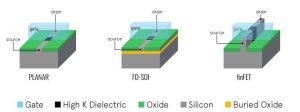
High performance and low power don’t really go together. For performance, the semiconductor industry moved to FinFET transistors some time ago, but the technology has only recently been pitched at ultra-low power applications. The majority of low-power technologies still rely on a planar transistor process, but FinFETs could be the next small thing in wearable technology.
Process technologies continue to evolve, with ultra-low power becoming one design objective
Power-saving circuit features
Saving power extends beyond process technology. Techniques continue to emerge, specifically intended to lower active power. Domino logic is not a new technology, but researchers continue to explore its low-power potential, particularly when used in a subthreshold process. Domino logic is related to dynamic logic, which uses a clock for combinatorial logic. This contrasts with static logic, which doesn’t use a clock.
Asynchronous logic extends the concept of clockless circuits. This approach uses a protocol between functional blocks to indicate when the result from one block is valid for the next, rather than synchronizing everything to a clock edge. The benefits of asynchronous logic were exploited when power density was becoming an issue. Removing the clock avoided the instantaneous surges in supply current that could occur when all functional blocks switched in time to a common clock. Research into how asynchronous logic could support lower supply rail voltages is ongoing.
Other techniques developed by processor manufacturers include voltage and clock scaling, which reduces both during times of low processor demand. This is still predominantly intended to address active power consumption, while standby, sleep and deep sleep modes are focused on static power. Techniques to reduce static power include clock and voltage gating, which removes the clock and/or supply rail from blocks of circuitry when they are not in use. With no power or signal to trigger switching, no power is consumed by the CMOS transistors in those areas.
ULP power management
Power management ICs, or PMICS, provide voltage regulation, conversion and supply protection in a single device. These features are important for most products, but they can be even more critical in battery-powered devices that strive for ultra-low power operation.
The features available from highly integrated PMICs include the standard protection that power management devices offer, such as over/under voltage/current protection, and short-circuit protection. PMICs aimed at rechargeable devices also include battery charging management, battery protection (thermal, deep discharge), and battery voltage monitoring during operation.
Additional features designed specifically for ultra-low power devices, such as wearables, include standby mode. This puts the PMIC itself into an ultra-low power mode, reducing the quiescent current when the wearable device isn’t being used.
In active mode, a highly integrated ultra-low power PMIC might include programmable buck and boost converters and low dropout regulators (LDOs) to supply all the product’s ICs even if they require different supply voltages. Supervisory features could include a watchdog circuit with power cycling, and a digital interface for communications with a host microcontroller. A PMIC can be an important part of an ultra-low power design strategy, as it will generally make the best use of the available energy in the battery and provide voltage gating.
Low-power display technologies
Light-emitting diode technologies continue to develop, offering higher pixel density and lower power. Active-matrix organic light emitting diode (AMOLED) technology has become popular with smartphone manufacturers and is expected to dominate foldable screens. Its use in wearables has also increased, with many smartwatches using AMOLED displays.
One of the most promising developments in recent years is the microLED array. The light output of a microLED, measured in Nits (candelas per m2) can be orders of magnitude higher than OLED technology. This means they need less power to provide the same Nits as other displays.
Just as with other displays, micro-LEDs are arrays of pixels based on three (red, green, blue) very small LEDs. Displays are manufactured using either a pick-and-place approach to position the micro-LEDs on a substrate or a monolithic process that doesn’t require the additional pick-and-place process. The monolithic microLED technology can support a smaller pixel pitch than pick-and-place technology. This makes it attractive for small wearable displays, in particular eyewear.
Other low-power display technologies include electronic paper. The main benefit of e-paper is its no-power operation. An e-display pixel works by suspending a pigment in an electrolyte. When polarized, the pigment’s orientation changes. Incident light is either reflected or passes through the pixel. A light source is needed to read the display, as the technology is not emissive, and the displays typically do not include a backlight. However, they are readable in direct sunlight, which makes them a popular choice for e-readers.
The main benefit of e-paper is that it is bistable, meaning no power is needed to retain the image on the screen. This makes it attractive for ultra-low power applications. As the technology develops, flexible solutions could find applications in smart clothing or wearables designed to be applied directly to the skin.
Ultra-low-power wireless communications
Wireless connectivity is not a prerequisite for wearable technology, as many applications could synchronize over a wired connection such as a docking station that also provides power to recharge batteries. However, consumer expectation has been set by early and current examples of wearables that offer an always-on, always-connected experience. It seems inevitable that wireless communication is now essential for future wearable technology.
Bluetooth remains the wireless technology of choice in peer-to-peer applications. While wearables may adopt a mesh networking model, the personal nature of wearable technology suggests that peer-to-peer will probably be favoured.
Recent revisions to the Bluetooth specification, from 5.0 onwards, have mostly focused on extending the applicability of Bluetooth to smart applications. These haven’t addressed power directly, but Bluetooth Low Energy, or BLE, (introduced with version 4.0) still manages to deliver excellent performance in ultra-low power applications.
If position tracking is an important feature of the wearable device, then Bluetooth version 5.1 onwards will be an attractive option. It includes location and tracking support by providing angle of arrival and angle of departure for the RF signal. This can be used to determine position when used with a beacon in a known location.
Some wearable devices may need to be directly addressable over the internet. Here, an IP-based mesh network protocol may be better. The options include 6LowPAN and Thread, as well as Wi-Fi. There are now several examples of system-on-chips that offer multi-protocol radios integrated alongside microcontroller cores to address this part of the wearables market.
Near-field communications (NFC) is another wireless technology making its way into the wearables sector. NFC can provide both power and data to a wearable sensor, to charge a small battery and exchange data. This would be a viable option for wearable devices that do not need to be always connected but are potentially always on.
The lab-on-a-chip for wearables
The idea of integrating digital processing alongside analog frontends for biomedical sensing has been around for some time. Developments continue in this area, with more focus on making medical devices wearable.
These highly integrated devices combine ultra-low power processing with dedicated sensor interfaces. This makes them less generic than most ICs, which is itself an indication that the market is maturing.
Optical sensors work well in this context, as they provide a non-invasive way of monitoring vital statistics and can be placed in various places around the body. Manufacturers are now integrating the photonic element alongside the logic to create a lab-on-a-chip solution. Again, the wrist is showing up as a favourite location for the wearable devices these ICs enable.
The future of wearable electronics
Forecasts for wearable technology have always been optimistic. The biggest potential has been and remains pinned on wearable technology for home health and medical applications. Integrated devices hold the key to enabling growth in the market and, as is normally the case, the IC manufacturers want to see the real potential before they invest too much time, money and effort into developing the solutions needed.
Once the decision has been made, it still takes time before those solutions appear. The dynamics of the semiconductor market can be frustrating for innovators and start-ups looking to launch a new application that will capture the minds of the end consumer. There are many such applications in the wearable space.
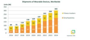
But there is proof positive that those solutions are now available. Smartwatches and fitness trackers are currently the primary examples of wearable technology, at least in the consumer sector, with sales continuing to expand. Medical devices are hugely interesting for manufacturers, but the market dynamics are clearly different. Augmented reality is primed to revolutionize the industrial vertical.
And this is perhaps the biggest challenge that wearable technology now faces. In terms of the end applications, it is hugely fragmented. Few other sectors face such a level of fragmentation. Fundamentally, however, the enabling technologies are largely the same. It falls to the OEM to leverage those technologies to create new products that really solve a problem or improve a situation in a specific application area.
Authored Article by: