


Introduction
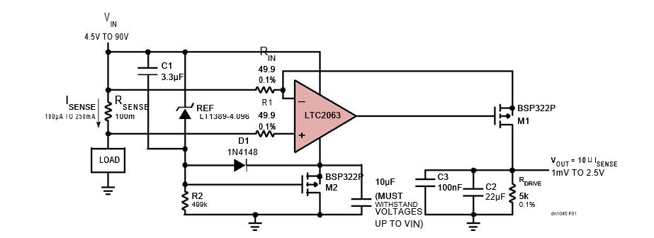
Precision high side measurement of microamp cur-rents requires a small value sense resistor and a low offset voltage amplifier. The LTC®2063 zero-drift amplifier has a maximum input offset voltage of just 5µV and draws just 1.4µA making it a great choice for building a complete ultralow-power precision high side current sense circuit, as shown in Figure 1.


This circuit uses only 2.3µA to 280µA of supply cur-rent to sense currents over a wide 100µA to 250mA dynamic range. The exceptionally low offset of the LTC2063 allows this circuit to work with only 100mΩ of shunt resistance, limiting the maximum shunt voltage to only 25mV. This minimizes power loss on the shunt resistor and maximizes power available to the load. The LTC2063’s rail-to-rail input allows this circuit to operate with very small load current where input common mode is almost at the rail. The integrated EMI filter of the LTC2063 protects it from RF interference in noisy conditions.
The voltage output of this circuit for a given sense current is:
VOUT = RDRIVER•RSENSE ISENSE = 10 •ISENSEIN
Zero Point
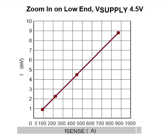
A critical specification for a current sense solution is the zero point, or equivalent error current at the input for the output produced when no sense current is present. The zero point is generally determined by the input offset voltage of the amplifier divided by RSENSE . The LTC2063’s low input offset voltage, of typical 1µV, maximum 5µV, and low typical input bias and offset currents of 1-3pA, allow for a zero point input-referred error current of only 10µA (1µV/0.1Ω) typically, or 50µA (5µV/0.1Ω) maximum. This low error allows the sense circuit to maintain its linearity down to the lowest current in its specified range (100µA), without plateauing due to loss of resolution, as seen in Figure 2. The resulting input current to output volt-age plot is linear over the entire current sense range.
Another source of zero point error is the output PMOS’s zero gate voltage drain current, or IDSS, a parasitic current that is present for nonzero VDS when the PMOS is nominally turned off (|VGS| = 0). A MOSFET with high IDSS leakage will produce a non-zero positive VOUT with no ISENSE.
The transistor used in this design, Infineon’s BSP322P, has an upper-bound IDSS of 1µA at |VDS| = 100V. As a good estimate for the typical IDSS of the BSP322P in this application, at room temperature, with VDS = –7.6V, IDSS is only 0.2nA, resulting in just 1µV error output, or equivalent 100nA input current error, when measuring 0A input current.
Architecture
The LT1389-4.096 reference, along with the bootstrap circuit composed of M2, R2, and D1, establishes a very low power isolated 3V rail (4.096V + V TH of M2, typically –1V) that protects the LTC2063 from seeing its absolute maximum supply voltage of 5.5V. Although a series resistance could suffice for establishing bias current, using transistor M2 allows for much higher overall supply voltages while also limiting current consumption to a mere 280µA at the high end of the supply range.
Precision
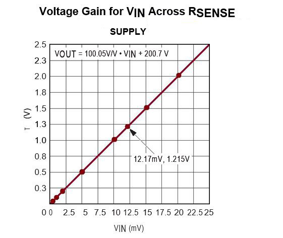
The LTC2063’s input offset voltage contributes a fixed input-referred current error of 10µA typical. Out of 250mA full-scale input, the offset results in only 0.004% error. At the low end, 10µA out of 100µA is 10% error. Since the offset is constant, it can be calibrated out. Figure 3 shows that total offset from LTC2063, unmatched parasitic thermocouples, and any parasitic series input resistances is only 2µV.
The gain shown in Figure 3, 100.05V/V is 1.28 greater than the expected gain given by the actual values of RDRIVE and RIN when built, or 4.978k/50.4 = 98.77V/V.
This error may be due to the different temperature coefficients of RDRIVE and RIN. The main source of uncertainty in the output of this circuit is noise, so filtering with large parallel capaci-tors is crucial to reduce noise bandwidth and thus the total integrated noise. With a 1.5Hz output filter, the LTC2063 adds about 2µVP -P low frequency, input-referred noise. Averaging the output over the longest possible duration further reduces error due to noise. Other sources of error in this current sense circuit are parasitic board resistance in series with the RSENSE at the LTC2063 input, tolerance in resistance values of the gain-setting resistors RIN and RDRIVE, mis-matched temperature coefficients in the gain-setting resistors, and error voltage at the op amp inputs due to parasitic thermocouples. The first three sources of error can be minimized by using Kelvin sense 4-lead sense resistors for RSENSE, and using 0.1% resistance with similar or low temperature coefficients for the critical gain- set path of RIN and RDRIVE. To cancel out the parasitic thermocouples at the op amp inputs, R1 should have the same metal terminals as RIN. Asym-metric thermal gradients should also be avoided as much as possible at the inputs.
The overall contribution of all the error sources dis-cussed in this section is at most 1.4% when referenced against full-scale 2.5V output, as shown in Figure 4.
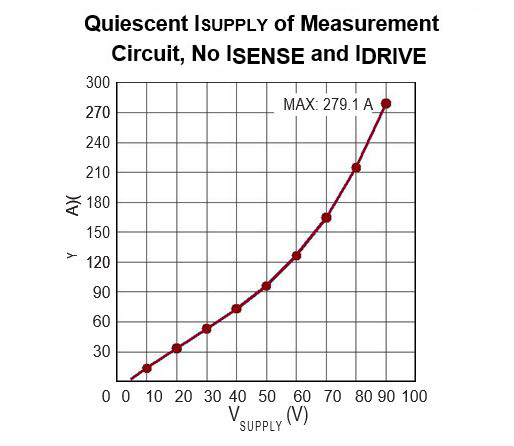
Supply Current
The minimum supply current required by the LT1389 and LTC2063 is 2.3µA at the minimum VSUPPLY and ISENSE (4.5V and 100µA), up to 280µA at maximum VSUPPLY and ISENSE (90V and 250mA), as shown in Figure 5. In addition to the current consumed by the active components, an output current IDRIVE through M1 also supplied by V SUPPLY is required, proportional to the output voltage, ranging from 200nA for a 1.0mV output (for 100µA ISENSE) to 500µA for a 2.5V output
Quiescent ISUPPLY of Measurement
Circuit, No ISENSE and IDRIVE
(for 250mA ISENSE). Thus, the total supply current in addition to ISENSE ranges from 2.5µA to 780µA. RDRIVE is set at 5kΩ for a reasonable ADC drive value.
Input Voltage Range
In this architecture, the maximum supply is set by the maximum |VDS| that the PMOS output can with-stand. The BSP322P is rated for 100V, so 90V is an appropriate operating limit.
Output Range
This design can drive a 5kΩ load, which makes it a suitable stage for driving many ADCs. The output voltage range is 0V to 2.5V. Since the LTC2063 has rail-to- rail output, the maximum gate drive is only limited by the LTC2063’s headroom. It is 3V typically in this design, set by the LT1389’s 4.096V plus the –1V typical VTH of M2.
Since the output of this circuit is a current, not a voltage, ground or lead offset does not affect ac-curacy. Thus, long leads can be used between the output PMOS M1 and RDRIVE, allowing RSENSE to be located near the current being sensed while RDRIVE is near an ADC and other subsequent signal chain stages. The drawback of long leads is increased EMI susceptibility. 100nF C3 across RDRIVE shunts away harmful EMI before it reaches the next stage’s input.
Speed Limits
Since the LTC2063’s gain- bandwidth product is 20kHz, it is recommended to use this circuit to measure signals 20Hz or slower. The 22µF C2 in parallel with the load filters the output noise to 1.5Hz for improved accuracy and protects the subsequent stage from sudden current surges. The trade-off of this filtering is longer settling time, especially at the lowest end of the input current range.
Conclusion
The LTC2063’s ultralow input offset voltage, low IOFFSET and IBIAS, and rail-to-rail input, provide pre-cise current measurements over the entire range of 100µA to 250mA. Its 2µA maximum supply current enables the circuit to run on far less than 280µA supply current for most of its operating range. Along with LTC2063’s low supply voltage requirements, the low supply current allows it to be powered from a voltage reference with headroom to spare.