


Every switch-mode power supply presents a wide-band noise source. Integrating a DC/DC converter from the car board net into an automotive control unit and still fulfilling the EMC requirements of automotive OEMs is a difficult task.
Typically, noise from the DC/DC converter and other high-speed circuits radiates via connected cables that provide an effective antenna path. To block this potential radiation path, filter circuitry is required at each cable connection point. This filtering is only effective if no H- or E-fields from the noise source couple into the filter components or cables.


In close-field environments, the amplitude of the fields falls by 1 over distance squared (1/d2). Therefore, a certain minimum distance is required between the noise source, filter components, and connector.
Unfortunately, PCB size and connector positions for the cables are usually pre-defined by mechanical constraints. Additionally, the maximum component height may be very limited in certain areas of the PCB, and two-sided assembly may not be possible. These conditions necessitate careful component placement and PCB layout—especially when working within highly regulated industries such as automotive manufacturing.
Real estate planning
To avoid directly coupling the E- and H-fields of the DC/DC converter into connectors and cables, the circuit must be placed as far from the PCB connection points as possible (Figure 1).
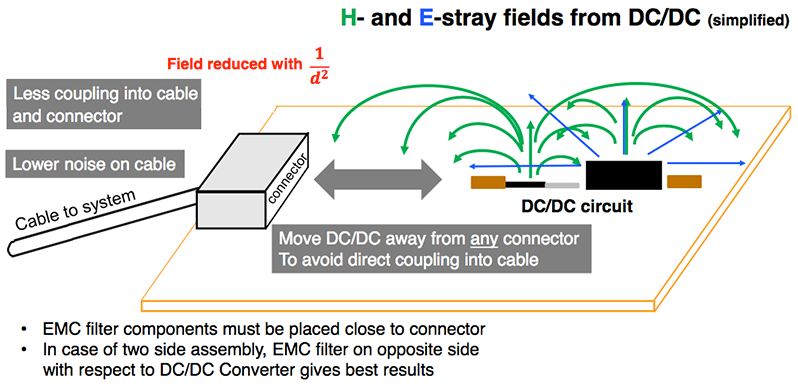 Figure 1 Place noise source max distance from connector and cable
Only distance or additional shielding can reduce the field strength at the EMC filters, connector, and cable to the necessary low levels. Shielding can replace distance!
It is best to use a two-side assembled PCB with at least four layers, where the DC/DC circuit and filter components are placed on opposite sides of the board. At least one inner layer should be solid GND to minimize cross-coupling from the noise source into the filter circuits.
In systems where the DC/DC circuit must be placed very close to the connector, effective shielding must be considered early in the design process. Thermally necessary heatsinks can sometimes be utilized for shielding. Ideally, the inductor, the DC/DC IC with power MOSFETs, and its decoupling capacitors are all located under the shield.
PCB layout guidelines
In a step-down converter, the main field sources are:
- High di/dt loop (hot loop), formed by the two power switches and CIN, which radiates wide-band magnetic fields
- SW node between power FETs and the inductor, with strong E-field radiation
- The inductor, which radiates E-fields and H-fields
AC-magnetic fields are shielded by solid metal areas that allow the induction of eddy currents. Due to its high conductivity, copper is very effective. Any conductor in the path of the potential difference that returns to a fixed potential on the PCB will effectively shield E-field radiation.
Any high di/dt loop radiates H-fields proportional to the loop area and current amplitude. Place the input capacitor close to the two power switches with a low-impedance connection to minimize the antenna loop area.
To further reduce the magnetic fields from this loop, place two sets of capacitors symmetrically at the power switches. Ideally, the peak currents in both loops will be half of the original, reducing the H-field by 6 dB. The orientation of the two loops is opposite, which further reduces the radiated H-field.
There should be a solid GND area in the layer under the DC/DC circuit, spaced with a distance of less than 100µm. In this copper area, the high di/dt currents flowing through the circuit components and PCB traces induce eddy currents. The eddy currents run opposite to the original currents on the component side, and their magnetic fields cancel the original field. This works best if the eddy current can mirror-image the high di/dt loop current from the component side with minimal distance. This reduces H-field radiation from the component side of the PCB. In an ideal case (super-conduction, zero distance, and perfect matching of both loop shapes), it would be canceled by the H-fields from the eddy currents.
Since the GND copper area under the DC/DC circuit has impedance, the high di/dt eddy currents create potential differences and make the area noisy. This noisy GND area must be separated from the system GND area, especially from any GND reference for filters and connectors. In a multi-layer PCB, these are separated by shaping the individual layers and by the impedance of the connecting vias between them.
A 3D view of the multi-layer PCB illustrates this concept (Figure 2).
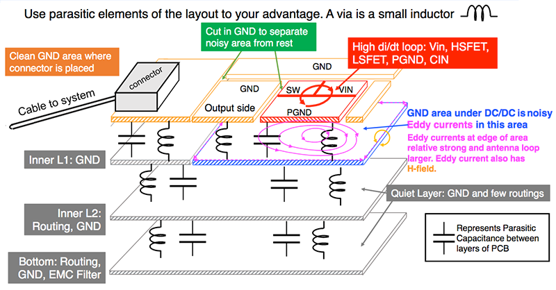 Figure 2 3D PCB view – layout is part of the circuit
On the top layer, the input capacitor (CIN) and the two power FETs join a VIN area and a PGND area (shown in red) that are connected to inner layers through vias. For the VIN path, the component after the vias must be an inductive element (e.g. a 1µH to 2µH coil). The high di/dt current from the switch transition is then forced to flow only in CIN, and not across the PCB.
The PGND area is not directly connected to any other GND on the component side, only through vias to the PGND area under the DC/DC block (shown in blue). The goal is to keep high-frequency currents on the component side, separating the noise from the “outside world.” At least one layer should be solid GND for the full size of the PCB to provide a low-impedance system reference. Remember, layout is part of the circuit.
Should copper be placed under the inductor?
Some PCB layout tools have a pre-setting that does not allow copper under an inductor core. Views on this topic range from no copper at all to copper directly under the coil on the component side of PCB.
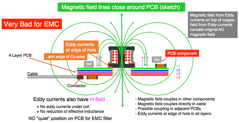
Figure 3 4-layer PCB with no copper under the coil
Figure 3 shows a sketch of the magnetic fields around the coil with no copper under the coil in any layer of a 4-layer PCB. The strong magnetic field lines from the coil are present on the bottom side of the PCB and close around the PCB, effectively coupling into any connected cable. Filter components on the PCB are bypassed through the air. This makes it very difficult, if not impossible, to meet automotive OEM EMC levels.
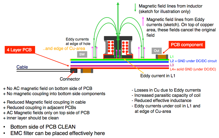 Figure 4 shows the PCB layout with copper directly under the coil on the component side.