


An increase in the component density of electronic items has revolutionised the entire electronics industry. In the quest of miniaturisation of devices, manufacturers have started finding new ways to increase the number of electronic devices on a single chip. This practise has evolved and taken us towards the nanometric regime. Nano Electronics has opened new avenues for designers that were previously unthinkable of. The article reviews this evolutionary change from micro to nano and also takes a look at some of the nanomaterials that are used in Nano Electronics.
With the invention of the first transistor, the entire semiconductor industry witnessed a monumental change. But, akin to human intelligence and nature, designers ramped up their pursuit to reduce the size of the transistor further in order to increase the number of transistors on a given chip. There simply was no stopping them. All this pursuit eventually led to the invention of computational circuits, and when Intel’s co-founder Gordon Moore said in 1965 that the number of transistors on an IC would double every two years, he was foreseeing the future of the entire electronics industry. Today, we know this prediction as the Moore’s law.


Moore’s law seems to have held its ground quite significantly until now, however, with the industry constantly demanding further miniaturisation of the modern semiconductor, it looks in jeopardy every passing day. There is perhaps only one thing that can potentially help in the sustenance of the law Nanoelectronics. You see, we have arrived at a point where miniaturisation yields more negatives than positives. So, the answer will have to come from the atomic level. The scaling down of transistors could not continue forever. The continued improvement in the communication and computational systems has been supported by miniaturization of devices on the chip. Scaling down of MOSFETs helps in sustaining the Moore’s law. The scaling down process reduces the power consumption. However, this scaling down can only be done up to a certain level. Scaling down of MOSFET below 50 nm leads to performance degradation.

Nano technology and Nano electronics
‘Nanotechnology’ term defined by Tokyo Science University Professor Norio Taniguchi in a 1974 paper, as follows: ‘Nano-technology’ mainly consists of the processing of, separation, consolidation, and deformation of materials by one atom or one molecule’. Nanotechnology refers to dealing with materials on a nanometric scale. These materials are studied on an atomic molecular level. Nanoelectronics refer to using nanotechnology in electronic components. By mixing the fields of chemistry, biology, physics and engineering, nanomaterials can be fabricated. It is also proposed that nanoelectronics will integrate devices at a smaller level. Richard Feynman gave a lecture on nanotechnology saying that, ‘There’s plenty of Room at the Bottom’. He suggested that materials can be manipulated at an atomic level.
Scaling down of transistors could not continue forever. Nanoelectronics may be able to continue this scaling down process. The idea of nanoelectronics was popularized in the 1980‟s, when work on resonant tunnelling and band gap engineering in low-dimensional semiconductor quantum wells and super lattices grew. This led to the creation of new opportunities for finding out the limits on the downscaling of conventional transistors. It is well known that when the size of a system becomes comparable to the electron wavelength, quantum effects become dominant. This occurs when transistors are downscaled and their characteristic dimensions reach the nanometre range, leading to new phenomena and possible novel devices based on quantum tunnelling mechanisms. For nanoelectronics to become a reality, it is essential that the new devices and circuits must be fabricated with nanometric precision.
Nanomaterials
According to Moore’s law the number of transistors on an IC would double up every two years. This has its own limitations; like greater complexity and heat dissipation. Apart from these limitations there are several other limitations that are imposed by silicon itself:
- Silicon has low mobility
- Silicon lattice absorbs some vibrations from transfer carriers, which converts to access heat.
- Shallow source/ Drain material – As transistors get smaller, doped wells are getting small that even ion implantation becomes difficult to control.
- Silicon gets contaminated at high temperature.
Therefore, silicon cannot be used at nano level. The various nanomaterials that have been discovered are:
- Carbon nanotubes
- Quantum Dots
- Single Electron Devices
Carbon Nanotubes
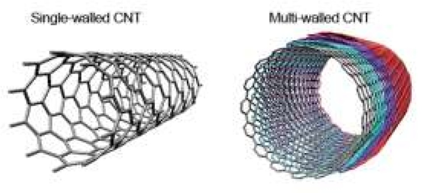
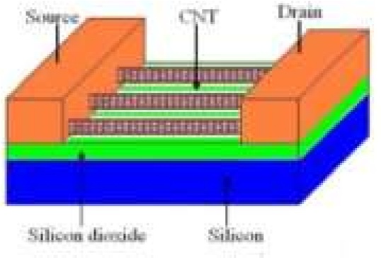
Carbon nanotubes, abbreviated as CNTs are seamless cylinders of carbon. These cylinders are formed by rolling of the graphene sheet into a tube. For clarity, imagine a chicken wire rolled into a tube. CNTs have transformed the electronic industry entirely; from large scale bulky systems to miniaturized systems. CNTs due to their wide range of properties, find use in many areas ranging from large scale automobile industry to nanometric scale electronics. Carbon nanotubes have extraordinary properties like small size and mass, high tensile strength and high thermal and electrical conductivities. These properties enable the use of CNTs in a number of applications. CNTs is categorize into two broad types; Single walled nanotubes (SWNTs) and Multiwall nanotubes (MWNTs). The electronic structure of nanotubes can be determined by the „Chirality Vector‟. CNTs due to their chirality, can be metallic or semiconducting. CNTs are used in making transistors called
CNT FETs. Nanotubes’s structure shows electrical properties due to unique and symmetric electronic structure of graphene. Nanotubes with smaller diameters show stronger electrical properties as compared to the nanotubes with larger diameters. CNTs are one dimensional conductors because of its nano scale cross section, electrons propagate only along the tube’s axis. Metallic nanotubes can carry an electric current density of 4 x 10^9 A/cm^2, which is more than 1000 times metals like copper. The strength of atomic bonds in carbon nanotubes allows them to withstand high temperatures. Hence, carbon nanotubes are very good thermal conductors. When compare to copper, commonly used as a thermal conductor, CNTs can transmit over 15 times more the amount of power (per meter per kelvin) than copper.
Quantum Dots
Quantum dot is stated as zero dimensional confined systems. Quantum dots are the semiconductors that have their dimensions in nanometric scale. These “quantum dots” obey the principle of quantum confinement. Quantum dots are the nano-particles having size from 10nm to 1000 nm. The term ‘Quantum Dots’ is made from the combination of two words – quantum and dot; because of their small size they are known as ‘Quantum’ and ‘Dots’ is due to their zero dimension. When the size of the semiconductor falls below the Bohr Radius then the material is called as Quantum Dot. The phenomena of quantum dot followed the older method of absorption and emission.
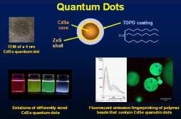
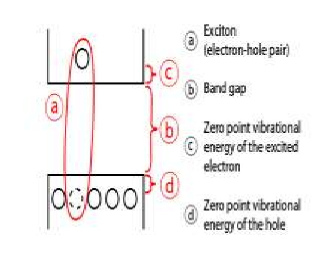
Quantum dots were discovered by Russian researcher Alexi Ekinov and Louis E. Brus. The mechanism of quantum dot states that with the absorption of energy, may it be in the form of heat or light, given to a semiconductor material; the electron will jump from the conduction band to valence band. This leaves behind a “hole” in the valence band. The hole and the electron together called as an ‘exciton’. The quantum dots are designed by the researchers by considering the properties of semiconductor material. When these excited electrons fall from their higher energy levels to the ground level, they emit energy in the form of light or heat. Quantum dot encodes the information by looking upon the position of the electron.
Single Electron Transistor (SET)
Due to the miniaturization of size in switching devices, the law of quantum mechanics cannot stay forever. Therefore, in order to solve this problem for semiconductor field, the single electron devices were developed. These artificially structured single electron transistors were studied to operate at low temperatures. But the molecular or atomic sized single electron transistor could function at room temperature.
Structure and Working
Due to small size, SETs have low power dissipation. Even at high speed the SET have low power dissipation. SET consist of two tunnel junctions sharing one common electrode with low self capacitance; that is known as island. The electrical potential of island can be tuned by a third electrode (the gate) capacitively coupled to the island. In blocking state, the energy is not accessible with tunnelling range of electron.
Simplified structure of SET
When a positive voltage is applied to the gate electrode, the energy levels of island electrode are lowered. The electron can tunnel onto the island. From there it can tunnel onto the drain electrode Fermi level. All the energy levels of island electrode are spaced by the separation of ∆ E. Basically, ∆E is the energy needed for each subsequential electron to island and to act as a self capacitance‘C’. As the value of capacitance decreases, the value of ∆ E increases. In other words, the capacitance and ∆E are inversely proportional to each other in a SET. Single electron devices are categorized as:
- Coulomb Blockade device. It is a SET device with three terminals based on coulomb blockade principle.
- Nano flash memory based devices. It also has three terminals but it is without tunnel barrier between source and drain.
- Yano type based devices. It is a two terminal device; information is stored in deep traps in poly-Si.
Conclusion
This article presents a comprehensive review of electronic components and their evolution from microelectronic and nano electronics regime. Nano electronics is the future of electronics. Nano electronics promises higher functionality with reduction in size. The various nano materials that have been discovered are faster, better and easy to handle. They display promising properties. Nanotechnology will give birth to new type of electronic components which are small in size, have lower power consumption and have increased functionality.