


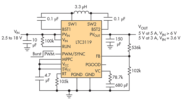
Linear Technology’s LTC3119 is an efficient, monolithic buck-boost converter that operates with inputs from 2.5 to 18 V (Fig. 1), making it well-suited to operate from one- to four-cell Li-ion batteries, unregulated wall adapters, solar panels, and supercapacitor inputs. The LTC3119’s tightly regulated output voltage can be programmed from 0.8 to 18 V.
Thanks to its low-RDS(ON) switches, the IC can supply 5-A output in buck mode. In boost mode, the step-up ratio (VOUT/VIN) reduces the amount of output current that it can support. The LTC3119 can supply 1.1 A of output for 3.6 VIN and 12 VOUT. For the same VIN, it’s capable of supporting an application requiring a 5-V, 3-A output.


Connecting a suitable resistor from the RT pin to ground sets an internal oscillator to switch from 400 kHz to 2 MHz. As a result, the system designer is able to trade off a slightly reduced conversion efficiency at higher switching frequency for a smaller solution size (specifically output capacitor and inductor size).
For noise-sensitive applications, an internal phase-locked loop (PLL) allows the switching frequency to be synchronized to an external clock. The PLL will acquire frequency lock with clock frequencies higher than the free-running frequency of the converter.
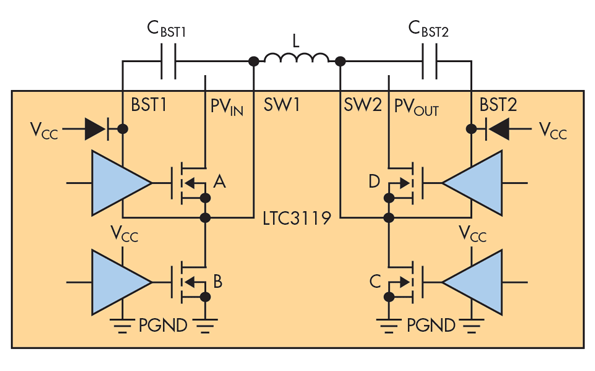
A proprietary, four-switch, pulse-width-modulation (PWM) buck-boost output stage in the LTC3119 (Fig. 2) provides low-noise, jitter-free switching through all operating modes, which is ideal for precision analog applications that are sensitive to power-supply noise. Integrated, low-RDS(ON), N-channel DMOS power switches minimize circuit complexity and maximize conversion efficiency.
High-side drive and sense circuitry enable current control and synchronous switch operation starting at 0 V on the output. Operation with inputs below 2.5 V is also possible by bootstrapping the VCC pin from VOUT, or other alternate sources—this enables maximum extraction of power from energy-storage devices such as supercapacitors.
In Operation
LTC3119 power switches operate continuously with currents up to their internal current-limit thresholds. Operating at high current levels results in significant heat generated within the IC. Give careful consideration to the thermal environment to optimize efficiency and ensure that the LTC3119 can provide its full-rated output current.
If the die temperature exceeds approximately 165°C, the IC will enter overtemperature shutdown and disable all switching. The IC will remain disabled until the die temperature cools by approximately 10°C. A soft-start circuit is re-initialized in overtemperature shutdown, providing a smooth recovery after removing the fault condition.
In PWM mode, the internal average-current control loop commands the pulse-width modulator to generate the appropriate switch duty cycle to maintain regulation of the output voltage. A proprietary ultra-low-noise PWM switching algorithm maintains output regulation with input voltages that are below, equal to, or above the output voltage. Transitions between buck and boost operating modes occur seamlessly without transients or subharmonic switching.
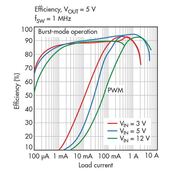
The user-selectable Burst Mode allows for high-efficiency operation at light loads and will automatically transition to the PWM mode at heavier loads. At low output currents, Burst Mode operation is enabled, with a current of only 31 μA (typical). In shutdown, the total supply current is further reduced to 3 μA (maximum). Fig. 3 shows a plot of efficiency for Burst Mode and PWM Mode operation.
Soft-Start
The LTC3119 soft-start circuit (Fig. 4) minimizes input-current transients and output-voltage overshoot on initial power-up. The required timing components for soft-start are internal to the LTC3119 and produce a typical soft-start duration of 6 ms. The internal soft-start circuit slowly ramps the command signal to the current-mode control loop (VC pin voltage). In doing so, the inductor current is also slowly increased, starting from zero. Soft-start is reset by the VCC UVLO, the RUN pin accurate enable comparator, and thermal shutdown.
To maintain a minimum input voltage, you can use the MPPC (maximum power point control) input of the LTC3119 with an optional external voltage divider to dynamically adjust the commanded inductor current. This is useful when using resistive sources, such as photovoltaic panels, to maximize input-power transfer and prevent VIN from dropping too low under load.
The MPPC pin is internally connected to the noninverting input of a transconductance amplifier. If the MPPC pin voltage falls below the reference voltage, the amplifier output reduces the commanded average inductor current (VC pin voltage) to reduce the input current and regulate VIN to the programmed minimum voltage.
An open-drain PGOOD output pulls low if VOUT falls more than 8% (typical) below its programmed value. When VOUT rises to within 6.5% (typical) of its programmed value, the internal PGOOD pull-down will turn off and PGOOD will go high if an external pull-up resistor is provided. An internal filter prevents nuisance trips of PGOOD due to short transients on VOUT. PGOOD can be pulled up to any voltage, as long as it doesn’t exceed the absolute maximum rating of 19 V.
The LTC3119 incorporates an average-current-mode control architecture consisting of two control loops. Both the inner average-current-mode control loop and outer control loop require compensation to maintain stability. The inner current-mode control loop is internally compensated to maintain wide bandwidth and good transient response. For many applications, the inner current loop can be treated like a voltage-controlled current source. This current source is commanded by the voltage error amplifier to regulate the output load formed primarily by the load resistance (RLOAD) and output capacitor (COUT).
External compensation may also be required, and is generally provided by a series resistor and capacitor connected between the MPPC pin and GND. This compensation network is in parallel with the lower resistor of the VIN voltage-divider network.
Capacitor Selection
A low-ESR (equivalent series resistance) output capacitor can minimize output-voltage ripple. Multilayer ceramic capacitors are an excellent option, as they maintain low ESR and come in small footprints. When choosing the capacitor value, it should be large enough to reduce the output-voltage ripple to acceptable levels.
Output-voltage ripple increases with load current and is generally higher in boost mode than buck mode. Besides the output-voltage ripple generated across the output capacitance, output-voltage ripple is also produced across the internal resistance of the output capacitor. The ESR-generated output-voltage ripple is proportional to the series resistance of the output capacitor.
The PVIN pin carries the full inductor current and provides power to internal control circuits in the IC. To minimize input voltage ripple and ensure proper operation of the IC, locate a low-ESR bypass capacitor with a value of at least 10 μF as close to this pin as possible. Keep the traces that connect this capacitor to PVIN and the ground plane as short as possible.
When powered through long leads or from a high-ESR power source, a larger-value bulk input capacitor may be required. In such applications, a 47- to 100-μF electrolytic capacitor in parallel with a 1-μF ceramic capacitor generally yields a high-performance, low-cost solution.
Inductor Selection
The choice of inductor impacts the maximum deliverable output current, converter bandwidth, magnitude of the inductor current ripple, and overall converter efficiency. The inductor must have a low dc series resistance (DCR), compared with the internal switch resistance (30 mΩ), or it will compromise output-current capability and efficiency.
With peak current-mode control, larger inductor values reduce inductor-current ripple but may not increase output-current capability. Larger-value inductors also tend to have a higher DCR for a given case size, which will have a negative impact on efficiency. Larger values of inductance will also lower the right-half-plane-zero (RHPZ) frequency when operating in boost mode, which can compromise loop stability.
Nearly all application circuits deliver the best performance with an inductor value between 1.5 and 15 μH. Buck-mode-only applications can use the larger inductor values since they aren’t affected by the RHPZ, while mostly boost applications generally require inductance on the lower end of this range, depending on the size of the step-up ratio. Regardless of inductor value, its saturation current rating should be selected to be greater than the worst-case average inductor current plus half of the ripple current.
PCB Layout
Because the LTC3119 switches large currents at high frequencies, pay special attention to the PCB layout to ensure a stable, noise-free, and efficient application circuit. Follow several key guidelines:
1. Minimize parasitic inductance and resistance of all circulating high-current paths. You can accomplish this by keeping the board traces to all components as short and as wide as possible. Capacitor ground connections should via down to the ground plane by way of the shortest route possible. The bypass capacitors on PVIN, PVOUT, and VCC should be placed as close to the IC as possible, and should have the shortest possible paths to ground.
2. The exposed pad is the electrical ground connection for the LTC3119. Multiple vias should connect the back pad directly to the ground plane. In addition, maximizing the metallization connected to the back pad will improve the thermal environment and improve the IC’s power-handling capabilities.
3. To minimize the cross-sectional area of the high-frequency current loops, there should be an uninterrupted ground plane under the entire converter. This shrinks EMI and reduces the inductive drops in these loops, thereby minimizing SW pin overshoot and ringing.
4. Make PCB trace connections to all components as wide as possible to reduce the series resistance. This will improve efficiency and maximize the output-current capability of the buck-boost converter.
5. To prevent large circulating currents in the ground plane from disrupting operation of the LTC3119, all small-signal grounds should return directly to GND by way of a dedicated Kelvin route. This includes the ground connection for the RT pin resistor, and the ground connection for the feedback network.
6. Keep the routes that connect to the high-impedance, noise-sensitive inputs FB and RT as short as possible to reduce noise pick-up.