


Introduction
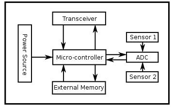
Wireless Sensor Networks consists of thousands of distributed nodes. These nodes are used for a wide range of applications like environmental monitoring-monitoring of air pollution, water quality, Forest fire detection, Landslide detection, Natural disaster prevention, Chemical sensing Health monitoring, Industrial monitoring – Machine health monitoring, Data logging, Data centre monitoring, Area monitoring- warfare etc. Each of these nodes are connected to one or more sensors. These sensors monitor the environment or the system by measuring various parameters like temperature, humidity, pressure etc. The nodes gather information and exchange it with other nodes or pass it to the sink node. Hence each node has to communicate with its neighbouring node. So every sensor node has the following blocks in it as shown in Fig. 1- transceiver, microcontroller, memory, sensors and power source.


When designing a node three characteristics has to be optimized- Small Size, Low power and Low cost. The Wireless Sensor sensor nodes are deployed in large number and they need to be managed for many years. Hence power consumption plays a vital role in wireless sensor networks as battery replacement is difficult and also costly. A sensor node has three main functions namely sensing, computation and communication. Out of these three functions the communication circuit consumes major percentage of the node energy . So the major challenge is to reduce the power consumption of the transceiver.
- Energy Model
A node can be said to remain in any of these states–sleep state, idle state and active state .The energy (Ei ) consumed by the node in any of these states depends on the power consumed (Pi ) by the circuit and the time (Ti) spent in that state. It is expressed as
Ei = Pix Ti
Active State
In this state the transceiver is turned on and is ready to communicate. It may be transmitting (Transmit State) or receiving (Receive State) data packets to or from the neighbouring nodes.
Transmit State
In this state, the transmitter circuit will be transmitting data to the nearby nodes and thereby consuming large power. Transmit state energy consumption is given by the equation
Etx = PtxxTtx
Where Ptx is the transmit power and Ttx is the transmit time.
Receive State
In this state, the receiver circuit receives data packet from the transmitter which is away by some distance. The energy consumed by the receiver when active is given by
Erx = (PrxxTrx) + Edecode
where Prx is the power consumption of the receiver circuit, Trx is the time taken
to receive the data and Edecode is the energy required to decode the data packet.
Idle State
In this state, the transceiver is active but not receiving or transmitting data packets. Hence most of the transceiver parts are active, and rest are switched off. The idle state power consumption of the transceiver is almost equal to that consumed in receive mode. Energy consumed in the idle state Eidle is given by
Eidle = Pidle x Tidle
Sleep State
Almost all parts of the transceiver are turned off in the sleep state. There are transceivers with different sleep states depending on the amount of circuits switched off. Energy in sleep state is given by
ESLP = PSLP x TSLP
where PSLP is due to the leakage power in the circuit and TSLP is the time spent in sleep state.
Transition States
Another state defined for a node is the transition state which is due to the power consumption during the activation and deactivation of electronic components whenever there is a transition between the states i and j. This state has a considerable energy consumption and hence has to be taken in to account. The energy consumed in transition state is given by
ESEij= Pij x Tij = Pji x Tji
It is assumed that Pij= Pji
The overall transceiver energy consumption is given by
Etransceiver = ( Etx + Erx + Eidle) + ESEij+ ESLP
Protocol based Duty Cycling
As wireless sensor networks are used for different applications with different data traffic. In most of the monitoring and sensing applications the amount of data to be transferred is very sparse and most of the time the node is idle. Hence one method to reduce power consumption is to duty cycle the node’s transceiver. In this method the node will be in sleep mode most of the time and will be on for small periods. So the active power consumption is considerably reduced. But a certain mechanism has to be provided to wake up the node to perform communication with the neighbour. In synchronous networks a common clock is given to all the nodes in the network. With this all nodes can communicate with each other in the assigned timeslots. But it is difficult to provide the common clock to all the nodes in the network.
An asynchronous method for communication between the nodes is using a wake up packet. The sensor nodes spend most of the time in sleep mode to reduce power consumption. When a transmitter wants to establish a connection with a node it sends a short wake up packet to the receiver. If the receiver is in active mode it sends an acknowledgement and establishes a connection. If the receiver is in sleep mode when the wake up packet arrives it cannot send the acknowledgement, so the transmitter transmits the wakeup packet till it receives an acknowledgement or it exhausts maximum number of attempts. This method eliminates the need for synchronization but increases the latency. To reduce latency the node is made to monitor the channel more often there by increasing the duty-cycle and the power consumption.
- Wake up Receiver
Another approach to reduce the power consumption in a node’s transceiver is to use a wake-up receiver. It is an additional receiver, that is used along with the main receiver. It overcomes the drawback of protocol based duty cycling . The wake up receiver continuously monitors the channel and on detecting a designated wakeup packet it activates the main receiver. The challenge is to design a wake up receiver whose active power consumption is low.
Wake-up Receiver Specification
Power consumption being the major criteria in the design of wake up receiver, other important factor considered is the sensitivity. Sensitivity is the minimum power at which the receiver can detect an RF signal and demodulate data. As the distance between the nodes increases the sensitivity of the signal has to increase. This increases the receiver power. For a wakeup receiver with low sensitivity the distance between the nodes is reduced. But this increases the number of nodes used in an area which results in the increase in implementation cost.
Data rate also plays a role in determining the receiver power. High data rate requires larger bandwidth and more power.
Wake up Receiver Architectures
Tuned-RF receiver Architecture
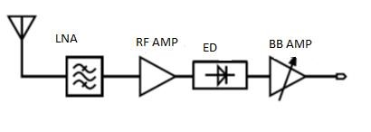
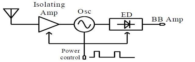
The tuned RF receiver shown in Fig. 2. has the following blocks. A low noise amplifier which is used to amplify the received weak RF signal. Demodulation of the RF signal is done by the envelop detector and is amplified by base band amplifier. As the low noise amplifier consumes a large percentage of the total power, removing it can reduce power by a great extent but at the loss of sensitivity. For a data rate of 100kb/s the receiver exhibits a sensitivity of – 53dBm with a power consumption of 12.5mW at 2.4GHz .
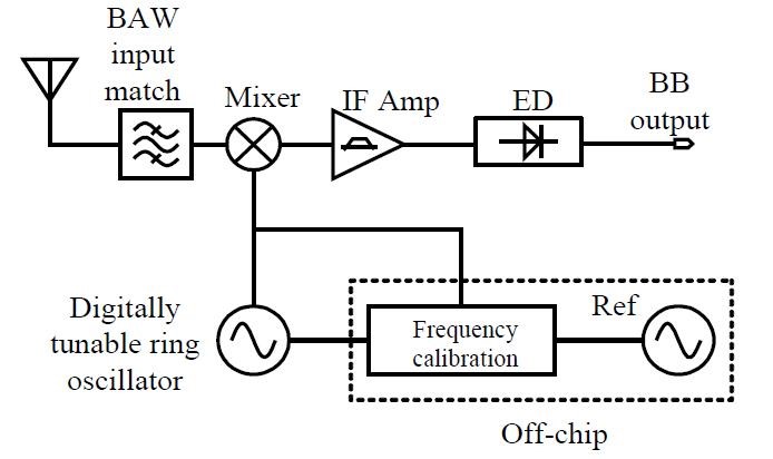
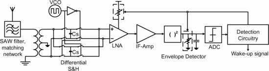
The architecture shown in Fig. 3.is a state of art receiver. This has a BAW resonator for filtering the input, a mixer for frequency conversion, an IF amplifier and an envelope detector. IF conversion is done as the processing of signal in the RF range consumes more power. The RF oscillator is replaced by a three stage CMOS ring oscillator. This architecture reports a power consumption of 52mW and sensitivity of -72dBm at a data rate of 100kb/s.
Tuned-RF with Double-Sampling
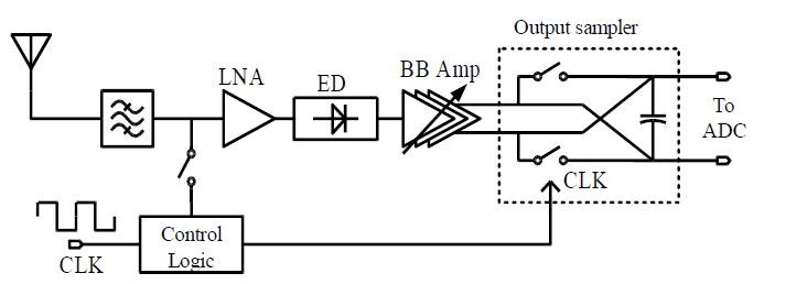
It is a slight modification to the tuned RF receiver where double-Sampling technique is employed as shown in Fig. 4. This double sampling down converts the RF signal to intermediate frequency that is greater than 1/f noise. Once again the intermediate frequency signal is down sampled to DC. The down sampling is done by a clock and a control logic. This reports a power consumption of 51mW and a sensitivity of -64dBm for the signal received at a data rate of 100kb/s.
Duty-cycled Architectures
Duty cycling is normally employed for power reduction. Depending upon the duty cycle, each block operates only for a small percentage of time. Hence even a power hungry block can be used in the duty cycled receiver with a minimum power consumption. The super-regenerative receiver shown in the Fig. 5.has a power consumption of 53mW with 10% duty-cycle and sensitivity of -75dBm at a data rate of 100kb/s with an operating frequency of 2.4GHz.
Duty Cycled Wakeup Receiver
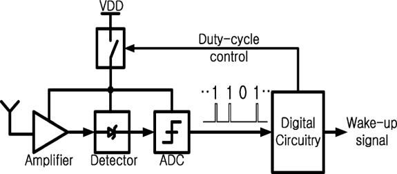
Though duty cycling reduces the power consumption it increases the latency of the network. The proposed wake up receiver in Fig. 6. reduces the power consumption and latency by adopting two different modes namely monitoring mode and identification mode . The start frame bit is received in monitoring mode and the rest of the wake up packet is transmitted in identification mode.
The data rates are also different for these modes. The wake up receiver monitors the channel for the start bit of the wake up packet. These bits are transmitted at a data rate of 1 kbps. The wake up receiver is duty cycled in this mode. On receiving the start bit the duty cycling is stopped and the wake up packet is transmitted at high data rate of 200kbps. The wake-up receiver consists of an amplifier, an envelope detector, an analog to digital converter and a digital circuitry to control the duty cycle. In the monitoring mode duty cycling is implemented by the use of a switch that gates the power to the wake up receiver. After receiving the start frame bit the switch is kept closed to receive the identification data in the identification mode. The proposed design achieves a sensitivity of 73 dBm, and the average power dissipation is 8.5 μW.
Dual Mode Wake up Receiver
In the receiver shown in Fig. 7. two modes are adopted namely monitoring mode and identification mode. In the monitoring mode the start frame bits are received and in identification mode the remaining wake up packet is received. By reducing the amplifier gain in the monitoring mode, power consumption is reduced. But this reduces the sensitivity. Hence to maintain the same sensitivity in monitoring mode and identification mode the data rate and bandwidth are lowered in the monitoring mode.
Conclusion
This paper presented the various architectures in implementing a low power wakeup receiver in a wireless sensor node. Of the architectures discussed the Un-certain IF reports a good sensitivity with considerably low power. In the duty cycled scheme the power consumption is reduced but with increase in latency. Hence by adopting different bandwidths for the monitoring mode and identification mode the power consumed by the circuit is still reduced.