


Description
This TI Design provides a compact solution capable of generating isolated DC power while supporting isolated RS-232 communication. The TIDA-01230 consists of a reinforced digital isolator with integrated power combined with an RS-232 communication module. The solution is designed in such a way as to take up minimal area to achieve this solution.


 Features
- Smallest Combination Solution (14.8 mm × 11.5 mm):
– Slightly Larger Than ISOW7842 Device Footprint
- Single Input Power Supply Solution:
– No Separate Isolated Supply Required to Power Interface-Side Components
- Reduced BOM Cost; Solution Eliminates Requirement for Separate Transformer
- Simpler Design
- Extendable to Other RS-232 Transceivers
Applications
• Grid Communication Modules
• Building Automation and HVAC
• Industrial Automation
• Remote Radio Unit (RRU) and Base Band Unit (BBU)
• Medical Equipment
• Other Communication Modules Dealing With High-Voltage Systems
 1 System Overview
1.1 Design Theory
1.1.1 Isolation in Data Communication
Most industrial interface systems are areas where noise can seriously affect the integrity of data transfer. A tested method of improving noise performance for any interface circuit is galvanic isolation. Isolating the low-voltage (LV) microcontroller (MCU) side from the high-voltage (HV) interface side has proven to be an effective solution to protect from data corruption and to protect LV side components from seeing HV stresses like electrostatic discharge (ESD), electrical fast transient (EFT), and surge.
Common-mode noise effects and many forms of radiated noise can affect the communication system.
Unwanted currents and voltages on a cable bus connecting multiple systems can cause severe problems.
These voltages and currents come primarily from two sources: ground loops and electrical line surges. Ground loops occur when a bus or system uses multiple ground paths. Two system grounds connected to the bus and separated by hundreds or thousands of meters may not have the same potential. Because of this potential difference, current flows between these points. This unintended current flow can damage or destroy components. Electrical surges can be caused by many sources, the result of currents coupled onto cable lines through induction. Long cable lines in industrial environments are especially susceptible to this phenomenon.
The operation of electric motors, in particular, causes rapid changes in the ground potential. These changes can generate a current flow through any nearby lines to equalize the ground potential. Other HV stress voltage sources include ESDs, coupled transient noises (EFT) and lightning strikes (surge). These induced surges can result in thousands of volts of potential on the line, and manifest themselves as transient current and voltage surges. Thus, a remote node may receive a 5- V switching signal superimposed on an HV level with respect to the local ground. These uncontrolled voltages and currents can corrupt the signal and be catastrophic to the device and system, damaging or destroying the components connected to the bus and resulting in system failure.
1.1.2 RS-232 Communication
The RS-232 communication protocol continues to withstand the test of time. Extensive use of the protocol for PLCs in industrial environments have started demanding RS-232 transceivers with smaller form factor, faster speed, lower power, cost efficiency, robustness, reliability, and ease of use. Higher speed and lower power come with reducing RS-232 voltage levels from ±12 V to ±5.4 V
Majority of RS-232 transceivers require compatibility with power supplies down to 3.3 V and use charge pumps to boost and invert that voltage to RS-232 voltage levels that are compatible with the standard > ±5 V.
The trend in recent years is to reduce power dissipation, especially in portable applications. Therefore, board designers have been reducing power-supply voltages or eliminating them altogether wherever possible. Lowering supply-voltage levels is a trait common to the semiconductor industry. Consequently, the burden of generating the necessary RS-232-compliant voltage swings is on the RS-232 driver IC. This can be accomplished with an internal or external charge pump or DC-DC converter. TI devices incorporate the RS-232 driver and charge pump in a single solution that makes it easy to design a circuit board using only a single supply.
1.2 System Description
The TIDA-01230 reference design combines both data and power isolation along with RS-232 communication interface to provide a robust, low-cost, low footprint solution that customers can directly place on their designs. This TI Design combines a High-Performance Reinforced Digital Isolator With Integrated High-Efficiency, Low Emissions DC-DC Converter (ISOW784x) with a Robust 3.3-V TwoChannel RS-232 Transceiver ( TRS3122E ).
The TIDA-01230 does not require any additional components to generate the isolated power. This makes the solution less than a quarter of the size of all existing solutions using a discrete transformer to generate the required isolated power. This TI Design takes a single power supply input (3 to 5.5 V) and digital signals referred to the input supply level. The board generates an isolated power supply using an integrated DC-DC converter. This isolated supply is used to power the RS-232 transceiver. The input signals are isolated and connected to the transceiver, which converts the digital signals into its RS-232 counterpart. Similarly, RS-232 signals fed at the transceiver end are converted to corresponding digital signals.
PLCs and grid communication systems have been an integral part of factory automation and industrial process control. They use digital and analog I/O modules to interface to sensors, actuators, and other equipment. Analog inputs for the PLC system include temperature sensors and transmitters, current sensors, voltage sensors, and others that can convert a physical quantity to an electrical signal. Digital inputs include push-buttons, proximity switches, photo sensors, pressure switches, and more. These signals need to be either group isolated or per channel isolated. PLCs are expected to work in harsh industrial environments. Hence sensor signals are converted to digital domain and coupled through a digital isolator to control domain. For sensor signal conditioning, power is generated from the backplane side by an isolated DC-DC converter. If multiple channels are present and all are isolated from each other, then use multiple of these isolated power solutions, which increase solution size and cost and bring down reliability due to increased component count. Fitting in the TIDA-01230 can significantly reduce the required area and bring down the BOM cost by eliminating the requirement for discrete transformers.
Medical equipment need isolation patient safety. For ECG, multiple leads are connected to the patient. The signal chain must be robust enough to capture very weak signals, digitize and process it, and pass it to the system controller over the isolation barrier. The power for signal processing units is typically generated by on board isolated DC-DC converters. This power can be replaced directly with the TIDA-01230 to get both communication and power isolation with the RS-232 interface. Also any peripheral connected to this equipment must be isolated from the controller. This solution makes sense to digitally isolate the interface signals and also power up the transceivers.
1.3 Key System Specifications
Table 1. Key System Specifications
| FEATURE | SPECIFICATION | VALUE |
| Input supply | Input voltage | 3 to 5 V |
| Isolated output supply | Output voltage | 3.3 V |
| Output current | 75 mA (3.3 VIN) | |
| 130 mA (5 VIN) | ||
| Communication | Max data rate | 1 Mbps (four channels) |
| Isolation | Clearance | > 3 mm |
| Working voltage | 300 VRMS | |
| CMTI | > 100 kV/µs | |
| EMI or EMC | ESD | 6 kV (across barrier) |
| 8 kV (on RS-232 lines) |
1.4 Block Diagram
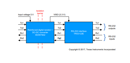
 Figure 1 shows the high-level block diagram of the TIDA-01230. As previously mentioned, this TI Design can be broken down into two main sections: the isolation block (ISOW7842) and the interface block ( TRS3122E ).
The TIDA-01230 works on a single input of 3 to 5.5 V. The integrated power supply can produce an isolated output voltage of 3.3 V (for any input) or 5 V (for VCC1 ≥ 5 V). This can be used to power up the RS-232 interface block. The TIDA-01230 communicates with digital signals on one side and gives the RS-232 lines on the other. The design can be interfaced to an MCU transmitting and receiving data using both channels (two for transmitting and two for receiving data). These signals are isolated from the RS232 lines available for communication to the field side. The side A of the isolator is powered from a 5-V or 3.3-V power supply, the secondary side of the isolator will be powered through the integrated isolated power supply. The integrated power supply can produce two voltage configurations on side B: 5 V or 3.3 V for the 5-V supply on side A, and 3.3 V for the 3.3-V supply on side A.
The load in this TI Design is the RS-232 transceiver. The design can interface with the MCU to transmit and receive data and enable transmission and reception. The signals to and from the MCU are isolated from the transceiver. The TIDA-01230 board can be broken down to two main sections: the isolation block and the interface block.
1.5 Highlighted Products
The TIDA-01230 features the following devices from Texas Instruments.
1.5.1 ISOW7842
The ISOW784x is a family of high-performance quad-channel reinforced digital isolators with an integrated high-efficiency power convertor. The integrated DC-DC convertor provides up to 650 mW of isolated power at high efficiency and can be configured for various input and output voltage configurations. These devices eliminate the need for a separate isolated power supply in space-constrained isolated designs. ISOW784x devices provide high electromagnetic immunity and low emissions, while isolating CMOS or LVCMOS digital I/Os. The signal isolation channel has a logic input and output buffer separated by a silicon dioxide (SiO2) insulation barrier, whereas power isolation uses on-chip transformers separated by a thin film polymer as insulation material. These devices prevent noise currents on a data bus or other circuits from entering the local ground and interfering with or damaging sensitive circuitry. Through innovative chip design and layout techniques, the electromagnetic compatibility of the ISOW784x has been significantly enhanced to ease system level ESD, EFT, surge, and emissions compliance. The high efficiency of the power convertor allows operation at a higher ambient temperature. The ISOW784x family of devices is available in a 16-pin SOIC wide-body (DWE) package.
• Integrated high-efficiency DC-DC convertor with on-chip transformer
- Wide input supply range: 3 to 5.5 V
- Regulated 5- or 3.3-V output
- Up to 0.65-W output power
- 130-mA load current (5 VIN to 5 VISO; 5 VIN to 3.3 VISO😉
- 75-mA load current (3.3 VIN to 3.3 VISO)
- Soft start to limit inrush current
- Overload and short-circuit protection
- Thermal shutdown
- Signaling rate up to 100 Mbps
- Low prop-delay: 13 ns typical (5-V supply)
- High CMTI: ±100 kV/µs min)
- Robust electromagnetic compatibility ( EMC )
- System level ESD, EFT, and surge immunity
- Low radiated emissions
- Safety-related certifications
- 7071-VPK Reinforced Isolation per DIN V VDE V 0884-10 (VDE V 0884-10): 2006-12
- 5000-VRMS Isolation for 1 Minute per UL 1577
- CSA Component Acceptance Notice 5A, IEC 60950-1 and IEC 60601-1 End Equipment Standards
- CQC Approval per GB4943.1-2011
- TUV Certification according to EN 60950-1 and EN 61010-1
- All agency certifications are planned
- Extended temperature range: –40°C to 125°C
1.5.2 TRS3122E
The TRS3122E is a two-driver and two-receiver RS-232 interface device, with split supply pins for mixed voltage operation. All RS-232 inputs and outputs are protected to ±15 kV using the IEC 61000-4-2 Air-Gap Discharge method, ±8 kV using the IEC 61000-4-2 contact discharge method, and ±15 kV using the human-body model. The charge pump requires five small 0.1-μF capacitors for operation from as low as a 1.8-V supply. The TRS3122E is capable of running at data rates up to 1000 kbps, while maintaining RS232- compatible output levels.
- Extended VCC operating nodes: 1.8 V, 3.3 V, or 5.0 V
- Unique tripler charge pump architecture enables low VCC of 1.8 V while maintaining compatibility with 3.3-V and 5-V supplies.
- Integrated level-shifting functionality eliminates the need for external power or additional level shifter while interfacing with low-voltage MCUs
- Enhanced ESD protection on RIN inputs and DOUT outputs
- ±15-kV IEC 61000-4-2 air-gap discharge
- ±8-kV IEC 61000-4-2 contact discharge
- ±15-kV human-body model
- Specified 1000-kbps data rate
- Auto powerdown plus feature
- Low 0.5-µA shutdown supply current
Meets or exceeds compatibility requirements of RS-232 interface
2 Getting Started Hardware
2.1 Board Description
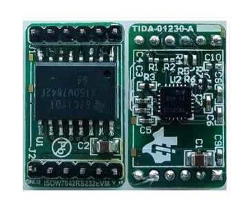
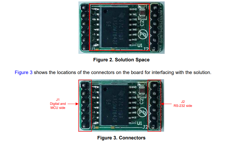
Figure 2 shows the size of the isolated RS-232 with an integrated power solution. The solution space within the board has been marked in red and is slightly bigger than the ISOW7842 IC. The board including all the connectors measures 21.1 × 12.7 mm while the actual solution space (marked in red) is 14.8 × 11.5 mm.
 2.2 Connectors Description
Table 2. Connectors
| CONNECTOR | PIN POSITION | PIN NAME | I/O OR
POWER |
DESCRIPTION |
| J1 | 1 | VIN | Power | Input supply (3 to 5.5 V) |
| 2 | Tx1 | I | Digital driver input | |
| 3 | Tx2 | I | Digital driver input | |
| 4 | Rx1 | O | Digital receiver output | |
| 5 | Rx2 | O | Digital receiver output | |
| 6 | GND1 | Ground | Input supply ground | |
| J2 | 1 | VISO | Power | Isolated power output |
| 2 | TxD1 | O | RS-232 output | |
| 3 | TxD2 | O | RS-232 output | |
| 4 | RxD1 | I | RS-232 receiver input | |
| 5 | RxD2 | I | RS-232 receiver input | |
| 6 | GND1 | Ground | Isolated output ground |
The design comes pre-populated with two of the TI ICs (ISOW7842 and TRS3122E). VIN and GND1 are connected at Pin 1 and Pin 6 of J1, respectively. Two channels are available for transmitting using RS-232 and two channels for receiving RS-232 signals. The digital inputs can be applied to Pin 2 and Pin 3 of J1 and the digital counterparts of the received RS-232 signals can be observed on Pin 4 and Pin 5 of J1. On the other side of the board, the corresponding RS-232 signals for the digital inputs from the MCU side can be observed at Pin 2 and Pin 3 of J2. Similarly, the RS-232 input signals can be given at Pin 4 and Pin 5 of J2. The boards include male berg heads to allow bus cables to be securely attached.
Connect MCU Tx lines to Pin 2 and Pin 3 of J1 and MCU Rx lines to Pin 4 and Pin 5 of J1. The corresponding RS-232 lines are available as four separate connections at J2, which can be connected directly to end system using required cables. The TI Design has four channels that can be used depending on the connections from the MCU side.
This TI Design can be extended to other RS-232 transceivers by replacing the existing transceiver on the board and selecting the right voltage configuration. The isolated output voltage configuration can be easily changed by changing the resistor combination of R1 and R2. See Table 3 to understand how to realize the required voltage configuration.
Table 3. Voltage Configurations
| INPUT VOLTAGE (V) | OUTPUT VOLTAGE (V) | R1 (Ω) | R2 (Ω) |
| 5.0 | 5.0 | Populate | Do Not Populate |
| 3.3 | Do Not Populate | Populate | |
| 3.3 | 3.3 | Do Not Populate | Populate |
| 5.0 | Invalid configuration | Invalid configuration |
3 Testing and Results
3.1 Test Setup
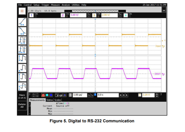
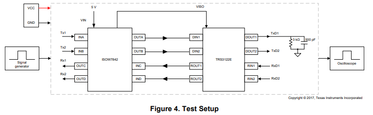 3.2 Communication Functionality
Waveforms were captured at max data rate from digital to RS-232 side.
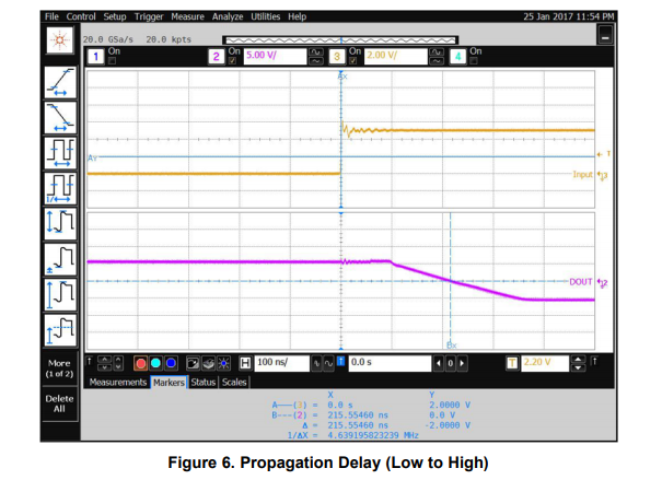
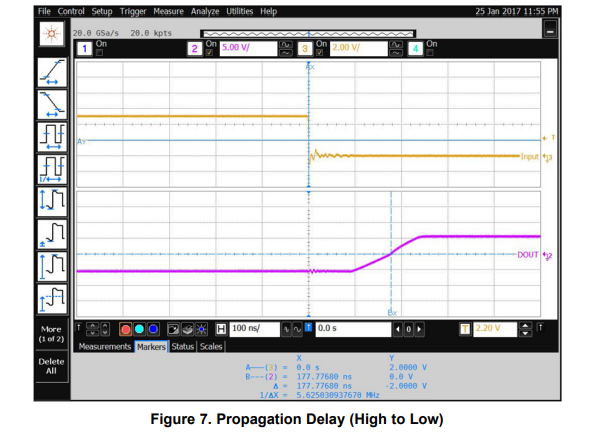
 3.3 Propagation Delay
 3.4 IEC-ESD Performance (IEC-61000-4-2)
Contact discharge IEC-ESD testing was performed on the TIDA-01230 using a pointed contact discharge tip. The board was subjected to mainly two kinds of ESD strikes. In the “Across barrier” row, the interface side was struck with the reference ground or power earth connected at the MCU side ground ( GND 1). Similarly for the “Same side” row, the interface lines were struck with the reference ground or power earth connected to the interface side ground (GND2). Table 4 shows the IEC-ESD test results. Each of the stressed pins were subjected to 10 strikes of each polarity of the corresponding stress voltage.
Table 4. IEC-ESD Results
| NATURE OF STRIKE | STRIKE POINT | STRESS VOLTAGE | RESULT |
| Across barrier | VISO | ±8 kV | Pass |
| TxD1 | ±8 kV | Pass | |
| TxD2 | ±8 kV | Pass | |
| RxD1 | ±8 kV | Pass | |
| RxD2 | ±8 kV | Pass | |
| GND2 | ±8 kV | Pass | |
| Same side | TxD1 | ±8 kV | Pass |
| TxD2 | ±8 kV | Pass | |
| RxD1 | ±8 kV | Pass | |
| RxD2 | ±8 kV | Pass |
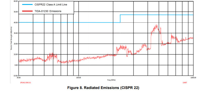
3.5 Radiated Emissions (CISPR 22)
The emission measurements were done according to CISPR 22 standards in a certified facility.Figure 8 shows the emissions measurement for the TIDA-01230 when the communication lines were being operated under a static high condition.
 Article Courtesy: Texas Instruments