


Description
This TI Design provides a compact solution capable of generating isolated DC power while supporting isolated RS-485 communication. The TIDA-00892 consists of a reinforced digital isolator with integrated power combined with an RS-485 transceiver. The solution is designed in such a way as to take up minimal area to achieve this.


 Features:
- Smallest Combination Solution: – Equal to ISOW7841 Device Footprint
- Smallest Combination Solution: – Equal to ISOW7841 Device Footprint
- Single Power Supply Solution: – No Separate Supply Required to Power the Interface-Side Components
- Reduced BOM Cost; Solution Eliminates Requirement For Separate Transformer
- Simpler Design
- Extendable to Other Full-Duplex RS-485 Transceivers: – SN65HVD14xx, SN65HVD7x, and SN65HVD3x
- Can Also be Extended to Half-Duplex With Minor Layout Changes
Applications:
- Grid Communication Modules
- Building Automation and HVAC
- Industrial Automation
- Medical Equipment
- Motor Drives
 1 System Overview
1.1 Design Theory
1.1.1 Isolation in Data Communication
Most industrial interface systems are areas where noise can seriously affect the integrity of data transfer. A tested method of improving noise performance for any interface circuit is galvanic isolation. Isolating the low-voltage (LV) microcontroller (MCU) side from the high-voltage (HV) interface side has proven to be an effective solution to protect from data corruption and to protect LV side components from seeing HV stresses like electrostatic discharge (ESD), electrical fast transient (EFT), and surge.
Common-mode noise effects and many forms of radiated noise can affect the communication system.
Unwanted currents and voltages on a cable bus connecting multiple systems can cause severe problems. These voltages and currents come primarily from two sources: ground loops and electrical line surges. Ground loops occur when a bus or system uses multiple ground paths. Two system grounds connected to the bus and separated by hundreds or thousands of meters may not have the same potential. Because of this potential difference, current flows between these points. This unintended current flow can cause bit errors and damage or destroy components.
Electrical surges can be caused by many sources, the result of currents coupled onto cable lines through induction. Long cable lines in industrial environments are especially susceptible to this phenomenon. The operation of electric motors, in particular, causes rapid changes in the ground potential. These changes can generate a current flow through any nearby lines to equalize the ground potential. Other HV stress voltage sources include ESDs, coupled transient noises (EFT) and lightning strikes (surge). These induced surges can result in thousands of volts of potential on the line and manifest themselves as transient current and voltage surges.
Thus, a remote node may receive a 5-V switching signal superimposed on a HV level with respect to the local ground. These uncontrolled voltages and currents can corrupt the signal and be catastrophic to the device and system, damaging or destroying the components connected to the bus and resulting in system failure. RS-485 systems that run over long distances and connect multiple systems are especially susceptible to these events.
Isolating the RS-485 system devices from each of the systems connected to the bus prevents ground loops and electrical surges from destroying circuits. Isolation prevents ground loops as each system connected to RS-485 cable bus and each RS-485 circuit has a separate and isolated ground. By referencing each RS-485 circuit only to one ground, ground loops are eliminated. Isolation also allows the RS-485 circuit reference voltage levels to rise and fall with any surges that appear on the cable line. Allowing the circuit voltage reference to move with surges, rather than being clamped to a fixed ground, prevents devices from being damaged or destroyed. To accomplish system isolation, both the RS-485 signal lines and power supplies must be isolated.
1.1.2 RS-485 Communication
Industrial and instrumentation applications (I and I) require transmission of data between multiple systems often over very long distances. The RS-485 bus standard is one of the most widely used physical layer bus designs in I and I applications.
The key features of RS-485 that make it ideal for use in I and I communications applications are:
- Long distance links of up to 4000 feet
- Bidirectional communications possible over a single pair of twisted cables
- Differential transmission increases noise immunity and decreases noise emissions
- Multiple drivers and receivers can be connected on the same bus
- Wide common-mode range allows for differences in ground potential between the driver and receiver
In harsh and noisy environments such as multi-unit residential buildings or industrial settings, an RS-485 bus architecture can be used to implement a low-cost, yet robust communications network. The differential nature of RS-485 signaling makes it less susceptible to external interference. Moreover, the RS-485 specification supports multidrop configurations, thus allowing the connection of multiple meters to a single bus. For instance, RS-485 can be used in an apartment building to transmit data from meters in each apartment to a central unit that aggregates the data from the individual meters, which can then be read through a wireless or PLC link. A similar approach can be used in industrial systems that require multiple cost centers to be metered.
1.2 System Description
The TIDA-00892 reference design combines both data and power isolation along with RS-485 communication interface to provide a robust, low-cost, low footprint solution that customers can directly place on their designs. This TI Design combines a High-Performance Reinforced Digital Isolator with Integrated High-Efficiency, Low Emissions DC-DC Converter (ISOW7841) with a Robust 3.3V Full-Duplex RS-485 Transceiver ( SN65HVD 1473).
The TIDA-00892 does not require any additional components to generate the isolated power. This makes the solution less than a quarter of the size of all existing solutions using a discrete transformer to generate the required isolated power. This TI Design takes a single power supply input (3 to 5.5 V) and digital signals referred to the input supply level. The board generates an isolated power supply using an integrated DC-DC converter. This isolated supply is used to power the RS-485 transceiver. The input signals are isolated and connected to the transceiver, which converts the digital signals into its RS-485 counterpart.
An electricity grid without adequate communications is simply a power broadcaster. It is through the addition of two-way communications that the power grid is made “smart.” Communications enables utilities to achieve three key objectives: intelligent monitoring, security, and load balancing. By using two-way communications, data can be collected from sensors and meters located throughout the grid and transmitted directly to the grid operator’s control room. This added communications capability provides enough bandwidth for the control room operator to actively manage the grid.
The communications must be reliable, secure, and cost effective. The sheer scale of the electrical grid network makes cost a critical consideration when implementing a communications technology. The communications used in grid infrastructure systems is dominated by RS-485. The TIDA-00892 design can fit in to power the RS-485 bus side and provide a cost-effective, low-footprint solution to this requirement.
PLCs and grid communication systems have been an integral part of factory automation and industrial process control. They use digital and analog I/O modules to interface to sensors, actuators, and other equipment. Analog inputs for the PLC system include temperature sensors and transmitters, current sensors, voltage sensors, and others that can convert a physical quantity to an electrical signal. Digital inputs include push-buttons, proximity switches, photo sensors, pressure switches, and more.
These signals need to be either group isolated or per channel isolated. PLCs are expected to work in harsh industrial environments. Hence sensor signals are converted to digital domain and coupled through a digital isolator to control domain. For sensor signal conditioning, power is generated from the backplane side by an isolated DC-DC converter. Fitting in the TIDA-00892 can significantly reduce the required area and bring down the BOM cost by eliminating the requirement for discrete transformers.
Medical equipment need isolation for patient safety. For ECG, multiple leads are connected to the patient. The signal chain must be robust enough to capture very weak signals, digitize and process it, and pass it to the system controller over the isolation barrier. The power for signal processing units is typically generated by onboard isolated DC-DC converters. This power can be replaced directly with the TIDA00892 to get both communication and power isolation with the RS-485 interface. Also any peripheral connected to this equipment must be isolated from the controller. This solution makes sense to digitally isolate the interface signals and also power up the transceivers.
1.3 Key System Specifications
Table 1. Key System Specifications
| FEATURE | SPECIFICATION | VALUE |
| Input supply | Input voltage | 3 to 5 V |
| Isolated output supply | Output voltage | 3.3 V |
| Output current | 75 mA (3.3 VIN) | |
| 130 mA (5 VIN) | ||
| Communication | Max data rate | 20 Mbps ( full-duplex communication) |
| Isolation | Clearance | > 3 mm |
| Working voltage | 300 VRMS | |
| CMTI | > 100 kV/µs | |
| EMI or EMC | ESD | 6 kV (across barrier) |
| 16 kV (across RS-485 lines) | ||
| Radiated emissions | CISPR22 (Class A) | |
1.4 Block Diagram
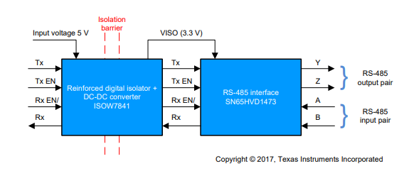
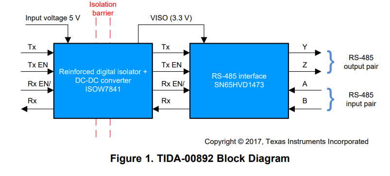 Figure 1 shows the high-level block diagram of the TIDA-00892. As previously mentioned, this TI Design can be broken down into two main sections: the isolation block (ISOW7841) and the interface block ( SN65HVD 1473).
The TIDA-00892 works on a single input of 3 to 5.5 V. The integrated power supply can produce an isolated output voltage of 3.3 V (for any input) or 5 V (for VCC1 ≥ 5 V). This can be used to power up the RS-485 interface block. The TIDA-00892 communicates with digital signals on one side and gives the RS485 lines on the other. The design can be interfaced to an MCU transmitting and receiving data while controlling the TX and RX enable lines. These signals are isolated from the RS-485 lines available for communication to the field side.
The SN65HVD1473 RS-485 transceiver and the isolated power supply integrated four channel digital isolator. The side A of the isolator is powered from a 5-V or 3.3-V power supply, the secondary side of the isolator will be powered through the integrated isolated power supply. The integrated power supply can produce two voltage configurations on side B: 5 V or 3.3 V for the 5- V supply on side A and 3.3 V for the 3.3-V supply on side A. The two available voltage configurations enable the same design to be used with other transceivers.
The load in this TI Design is the RS-485 transceiver. The design can interface with the MCU to transmit and receive data and enable transmission and reception. The signals to and from the MCU are isolated from the transceiver. The TIDA-00892 board can be broken down to two main sections: the isolation block and the interface block.
1.5 Highlighted Products
The TIDA-00892 features the following devices from Texas Instruments.
1.5.1 ISOW7841
The ISOW784x is a family of high-performance quad-channel reinforced digital isolators with an integrated high-efficiency power convertor. The integrated DC-DC convertor provides up to 650 mW of isolated power at high efficiency and can be configured for various input and output voltage configurations. These devices eliminate the need for a separate isolated power supply in space-constrained isolated designs. ISOW784x devices provide high electromagnetic immunity and low emissions, while isolating CMOS or LVCMOS digital I/Os.
The signal isolation channel has a logic input and output buffer separated by a silicon dioxide (SiO2) insulation barrier, whereas power isolation uses on-chip transformers separated by a thin film polymer as insulation material. These devices prevent noise currents on a data bus or other circuits from entering the local ground and interfering with or damaging sensitive circuitry. Through innovative chip design and layout techniques, the electromagnetic compatibility of the ISOW784x has been significantly enhanced to ease system level ESD, EFT, surge, and emissions compliance. The high efficiency of the power convertor allows operation at a higher ambient temperature. The ISOW784x family of devices is available in a 16-pin SOIC wide-body (DWE) package. Integrated high-efficiency DC-DC converter with on-chip transformer.
- Wide input supply range: 3 to 5.5 V
- Regulated 5- or 3.3-V output
- Up to 0.65-W output power
- 130-mA load current (5 to 5 V; 5 to 3.3 V;)
- 75-mA load current (3.3 to 3.3 V)
- Soft start to limit inrush current
- Overload and short circuit protection
- Thermal shutdown
- Signaling rate up to 100 Mbps
- Low prop-delay: 13 ns typical (5-V supply)
- High CMTI: ±100 kV/µs ( min )
- Robust electromagnetic compatibility ( EMC )
- System level ESD, EFT, and surge immunity
- Low radiated emissions
- Safety-related certifications
- 7071-VPK Reinforced Isolation per DIN V VDE V 0884-10 (VDE V 0884-10): 2006-12
- 5000-VRMS Isolation for 1 Minute per UL 1577
- CSA Component Acceptance Notice 5A, IEC 60950-1 and IEC 60601-1 End Equipment Standards
- CQC Approval per GB4943.1-2011
- TUV Certification according to EN 60950-1 and EN 61010-1
- All agency certifications are planned
- Extended temperature range: –40°C to 125°C
1.5.2 SN65HVD1473
The SN65HVD1473 is a full-duplex transceiver that features the highest ESD protection in the RS-485 portfolio, supporting ±16-kV IEC61000-4-2 contact discharge and > ±30-kV HBM ESD protection. This RS485 transceiver has a robust 3.3-V driver and receiver and is offered in a standard SOIC package as well as in a small-footprint MSOP package. The large receiver hysteresis of the SN65HVD1473 device provides immunity to conducted differential noise and the wide operating temperature enables reliability in harsh operating environments.
This device combines a differential driver and a differential receiver, which operate from a single 3.3-V power supply. Each driver and receiver has a separate input and output pins for full-duplex bus communications designs. These devices all feature a wide common-mode voltage range which makes the devices suitable for multi-point applications over long cable runs.
The SN65HVD1473 device has active-high driver enables and active-low receiver enables. A low, less than 5-µA standby current can be achieved by disabling both the driver and receiver.
- 1/8 unit-load options available
- Up to 256 nodes on the bus
- Bus I/O protection
- >±30-kV HBM protection
- >±16-kV IEC-61000-4-2 Contact Discharge
- >±4-kV IEC61000-4-4 Fast Transient Burst
- Extended industrial temperature range:
- –40°C to 125°C
- Large receiver hysteresis (70 mV) for noise rejection
- Low power consumption
- <1.1-mA quiescent current during operation
- Low standby supply current: 10 nA typical, < 5 µA ( max )
- Glitch-free power-up and power-down protection for hot-plugging applications
- 5-V tolerant logic inputs compatible with 3.3-V or 5-V controllers
2 Getting Started Hardware
2.1 Board Description
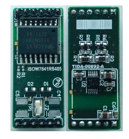
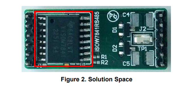
Figure 2 shows the size of the isolated RS-485 with an integrated power solution. The solution space within the board has been marked in red and is slightly bigger than the ISOW7841 IC. The full board measures 31 × 13.3 mm while the actual solution space (marked in red) is 11.9 × 11.2 mm.
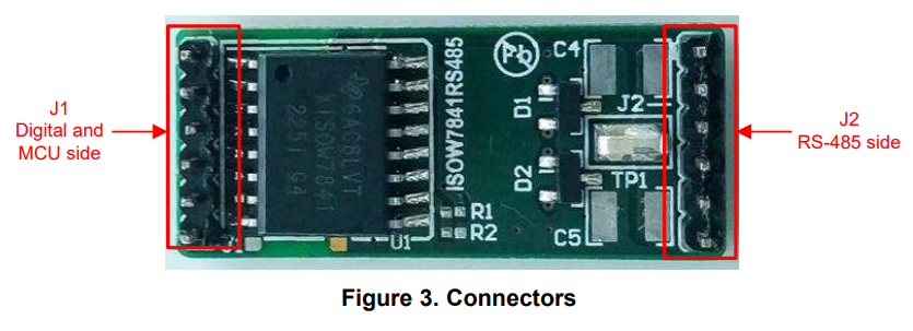
2.2 Connectors Description
Table 2. Connectors
| CONNECTOR | PIN POSITION | PIN NAME | I/O OR POWER | DESCRIPTION |
| J1 | 1 | VIN | Power | Input supply (3 to 5.5 V) |
| 2 | Tx | I | Digital driver input | |
| 3 | Tx EN | I | Driver enable | |
| 4 | Rx EN/ | I | Receiver enable | |
| 5 | Rx | O | Digital receiver output | |
| 6 | GND1 | Ground | Input supply ground | |
| J2 | 1 | VISO | Power | Isolated power output |
| 2,3 | Y, Z | O | RS-485 output pair | |
| 5,4 | A, B | I | RS-485 input pair | |
| 6 | GND2 | Ground | Isolated output ground |
The design comes pre-populated with two of the TI ICs (ISOW7841 and SN65HVD1473) and a 120-Ω termination resistor on the bus to match the transmission line impedance. VCC1 and GND1 are connected at Pin 1 and Pin 6 of J1, respectively. The digital input can be applied to Pin 2 of J1 and the receiver output can be observed on Pin 5 of J1. On the other side of the board, the differential bus lines A and B (RS-485 input lines) are Pin 5 and Pin 4 respectively on J2, while Y and Z (RS-485 output lines) are connected to Pin 2 and Pin 3 respectively on J2. The boards include male berg heads to allow bus cables to be securely attached.
Connect MCU Tx to Pin 2 of J1 and MCU Rx to Pin 5 of J1. Connect the driver and receiver enable lines from MCU to Pins 3 and 4, respectively. The RS-485 lines, AB and YZ, need to be connected as individual pairs of twisted pair cables. The system can be configured and used for half-duplex or full-duplex communication by providing appropriate transmit and receive enable signal from MCU side.
This TI Design can be extended to other RS-485 transceivers by replacing the existing transceiver on the board and selecting the right voltage configuration. The isolated output voltage configuration can be easily changed by changing the resistor combination of R1 and R2. See Table 3 to understand how to realize the required voltage configuration.
Table 3. Voltage Configurations
| INPUT VOLTAGE (V) | OUTPUT VOLTAGE (V) | R1 (Ω) | R2 (Ω) |
| 5.0 | 5.0 | Populate | Do Not Populate |
| 3.3 | Do Not Populate | Populate | |
| 3.3 | 3.3 | Do Not Populate | Populate |
| 5.0 | Invalid configuration | Invalid configuration |
3 Testing and Results
3.1 Test Setups
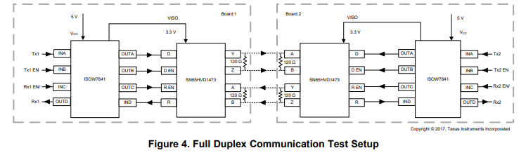
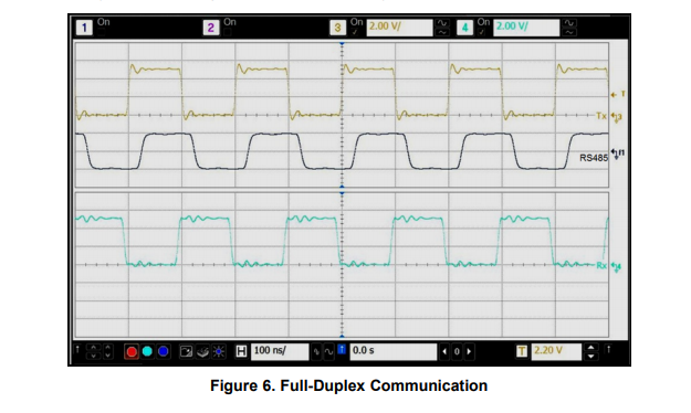
 3.2 Full-Duplex Communication
As shown in Figure 4, two boards are connected to each other, forming a full-duplex system for the test setup. Both the boards are powered with a 5-V supply voltage and VISO is configured for 3.3 V in a fullduplex mode (Tx EN pulled high and Rx EN pulled low).
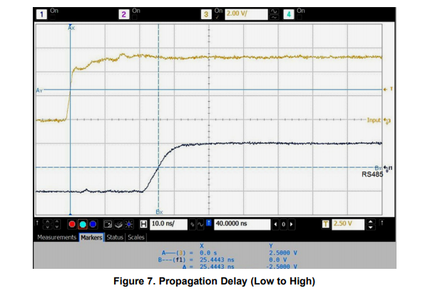
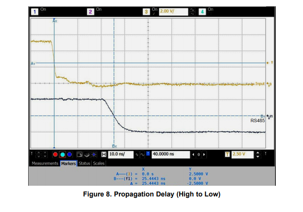
 3.3 Propagation Delay
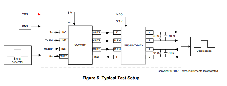
As shown in Figure 5, single board propagation delay from digital side to RS-485 side was measured.
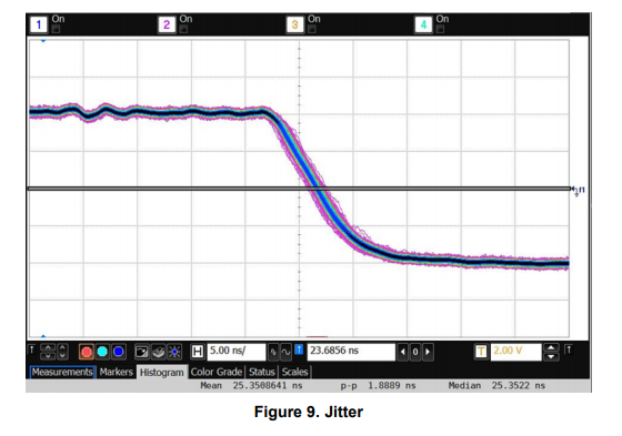
 3.4 Jitter
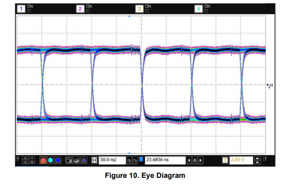
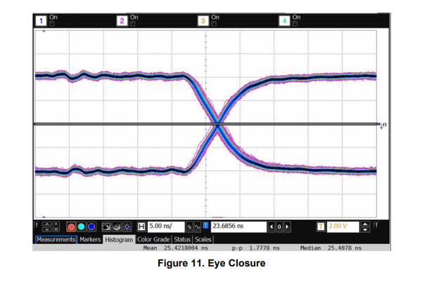
 3.5 Eye Diagram
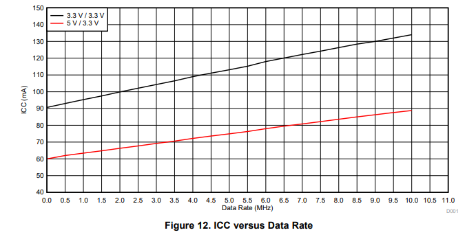
 3.6 Current Consumption
Current consumption of the TIDA-00892 was measured with both the RS-485 receiver and transmitter toggling at different data rates. Termination resistors were populated as per Figure 5.
 3.7 IEC-ESD Performance (IEC-61000-4-2)
Contact discharge IEC-ESD testing was performed on the TIDA-00892 using a pointed contact discharge tip. The board was subjected to mainly two kinds of ESD strikes. In the “Across barrier” row, the interface side was struck with the reference ground or power earth connected at the MCU side ground ( GND 1). Similarly for the “Same side” row, the interface lines were struck with the reference ground or power earth connected to the interface side ground (GND2). Table 4 shows the IEC-ESD test results. Each of the stressed pins were subjected to 10 strikes of each polarity of the corresponding stress voltage.
Table 4. IEC-ESD Results
| NATURE OF STRIKE | STRIKE POINT | STRESS VOLTAGE | RESULT |
| Across barrier | VISO | ±6 kV | Pass |
| Y | ±6 kV | Pass | |
| Z | ±6 kV | Pass | |
| A | ±6 kV | Pass | |
| B | ±6 kV | Pass | |
| GND2 | ±6 kV | Pass | |
| Same side | Y | ±16 kV | Pass |
| Z | ±16 kV | Pass | |
| A | ±16 kV | Pass | |
| B | ±16 kV | Pass |
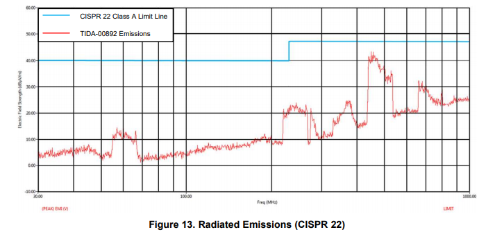
3.8 Radiated Emissions (CISPR 22)
The emissions measurements were done according to CISPR 22 standard in a certified facility. Figure 13 shows the emissions measurement for the TIDA-00892 design when the communication lines were being operated under a static high condition.
Article Courtesy: Texas Instruments