


Allegro MicroSystems, LLC is a world leader in developing, manufacturing, and marketing high-performance Hall-effect sensor integrated circuits. This note provides a basic understanding of the Hall effect and how Allegro designs and implements Hall technology in packaged semiconductor monolithic integrated circuits.
Hall Effect Principles


The Hall effect is named after Edwin Hall, who in 1879 discovered that a voltage potential develops across a current carrying conductive plate when a magnetic field passes through the plate in a direction perpendicular to the plane of the plate, as illustrated in the lower panel of figure 1.
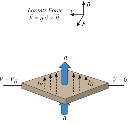 The fundamental physical principle behind the Hall effect is the Lorentz force, which is illustrated in the upper panel of figure 1. When an electron moves along a direction, v, perpendicular to the applied magnetic field, B, it experiences a force, F, the Lorentz force, that is normal to both the applied field and the current flow.
In response to this force, the electrons move in a curved path along the conductor and a net charge, and therefore a voltage, develops across the plate. This Hall voltage, VH, obeys the formula below, which shows that VH is proportional to the applied field strength, and that the polarity of VH is determined by the direction, either north or south, of the applied magnetic field. By this property, the Hall effect is employed as a magnetic sensor.
![]()
where,
VH is the Hall voltage across the conductive plate,
I is the current passing through the plate,
q is the magnitude of the charge of the charge carriers, ρn is the number of charge carriers per unit volume,
and t is the thickness of the plate.
Allegro semiconductor integrated circuits integrate a Hall element, as the Hall effect applies to both conductive plates and semiconductor plates. By using the Hall effect in a fully integrated monolithic IC it is possible to measure magnetic field strength and create a vast array of Hall-effect integrated circuits for many different applications.
An Allegro Hall switch is activated by a positive magnetic field that is generated by a south pole. A positive field will turn on the output transistor and connect the output to GND, acting as an active low device.
The field required to activate the device and turn on the output transistor is called the magnetic operating point, and is abbreviated BOP. When the field is removed the output transistor is turned off. The field required to turn off the device once it is activated is called the magnetic release point, or BRP. The difference between BOP and BRP is called the hysteresis and is used to prevent switching bounce due to noise.
Allegro also makes magnetic latches and linear devices. Magnetic latches switch on with a south pole (BOP) and switch off with a north pole (BRP). Requiring a north pole to deactivate the latch separates latches from simple switches. Because they do not switch off when the field is removed, they “latch” the output in the present state until the opposite field is applied. Latches are used for sensing rotating magnets for motor commutation or speed sensing.
Linear devices have an analog output and are used for linear position sensing in linear encoders such as automotive throttle pedal position sensors. They have a ratiometric output voltage that is nominally VCC / 2 when no field is applied. In the presence of a south pole the output will move in the direction of VCC and in the presence of a north pole the output will move in the direction of GND. Allegro has a broad range of Hall switches, latches and linear devices suitable for a wide variety of applications.
Please reference the Allegro product selection guide at: http://www.allegromicro.com/en/Products/Categories/Sensors
Employing the Hall Effect
Allegro Hall-effect integrated circuits (IC) employ the Hall effect by incorporating a Hall element with other circuitry, such as opamps and comparators, to make magnetically activated switches and analog output devices. A simple Hall switch, such as the open NMOS device shown in figure 2, can be used to determine if a magnet is present or absent, and responds with a digital output.
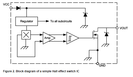 Integrated circuits are electronic structures having a large number of circuit elements in high density, regarded as a single unit. The circuit elements include active components such as transistors and diodes, as well as passive components such as resistors, capacitors, and inductors. These components are interconnected by metal, usually aluminum, to make up the more complex op-amps and comparators of the device. The Hall switch in figure 2 is used for a simple illustration, but these components are employed on all Allegro devices for even the most complex ICs. The Hall element in figure 2 is shown as the square box with the “X.” Its output is amplified, fed into a comparator, and then to an open NMOS digital output. Allegro also makes Hall ICs with two Hall elements for sensing differential magnetic fields and even three Hall elements for direction detection of moving ferromagnetic targets. However complex the sensor topology, the components are all manufactured in and on the surface of a thin substrate of a semiconductor material.
Hall IC Structure
Allegro devices are manufactured on silicon substrates, by doping directly into the silicon with different materials to create n-type (electron) or p-type (electron hole) carrier regions. These n-type and p-type material regions are formed into geometries that make up the active and passive components of the integrated circuit, including the Hall element, and are connected together by depositing metal over the geometries. In this way the active and passive components are electrically connected together. Since the geometries required are very small, in the range of microns and sometimes even smaller, the circuit density is extremely high, allowing complex circuits on a very small area of silicon.
The fact that all the active and passive elements are grown within the substrate, or deposited on the silicon, makes them inseparable from the silicon, and truly identifies them as monolithic integrated circuits. Figure 3 shows how a Hall element is integrated into the Allegro IC. It is simply an area of doped silicon that creates an n-type plate that will conduct current.
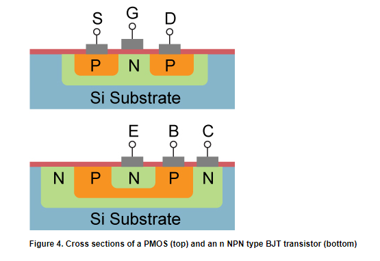
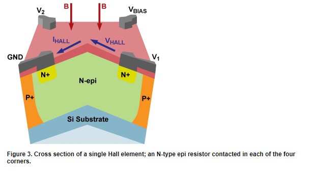 As mentioned earlier, when a current is forced from one corner of the plate to the opposite corner, a Hall voltage will develop across the other two corners of the plate when in the presence of a perpendicular magnetic field. The Hall voltage will be zero when no field is applied. In a similar fashion more complex geometries make up active components such as NPN or NMOS transistor structures. Figure 4 shows cross-sections of both NPN and PMOS transistors.
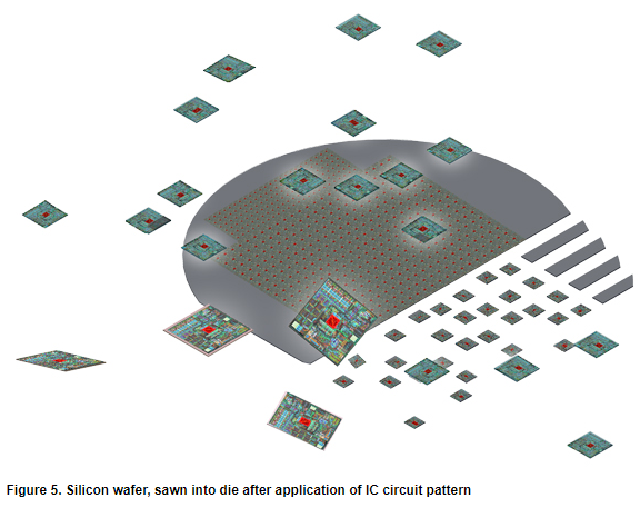
 For production efficiency, these circuits are grown in the substrate while it is still in the form of a large wafer. The circuits are repeated in a pattern of rows and columns that can be sawn into individual die, or “chips,” as illustrated in figure 5.
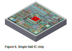
 A single Allegro Hall-effect sensor IC device can be seen in figure 6. This is the simple switch with functional block diagram as shown in figure 2. All of the circuitry is included on the IC, including the Hall element which can be seen as the red square in the middle of the chip, as well as the amplifier circuitry and protection diodes and the numerous resistors and capacitors needed to realize the device functionality.
Hall Device Packaging
After sawing the silicon wafer rows and columns into individual die, the die are then packaged for individual sale. A completed package, one of many possible styles, is shown in figure 7. The die is seen inside the case, mounted on a copper die pad. Contact to the copper leads is made through gold wire-bonding from metal pads on the die surface to the electrically isolated package leads. The package is then encapsulated, or overmolded, with plastic to protect the die from damage.
 The package in figure 7 is the simple switch of figure 2 with VCC, GND, and an Output leads in a miniature 3-pin single inline package (SIP). Other packages can be seen in figure 8 and include a wafer-level chip scale package (CSP), an SOT23W, an MLP, a 3-pin UA-package SIP, and a 4-pin K-package SIP.
