


 technology can further enhance that level of protection when used by chips that implement cryptographic functionality.)
Abstract
Hardware-based security provides robust protection against cyberattacks, and physically unclonable function (PUF) technology can further enhance that level of protection when used by chips that implement cryptographic functionality. This application note discusses a new PUF semiconductor solution that utilizes the random analog characteristics of MOSFET transistors, the fundamental building block of CMOS ICs. At the chip level, the PUF solution is constructed from an array of analog circuit elements, featuring inherent randomness in I-V characteristics and sized according to the number of bits required to achieve the cryptographic requirements of the chip. When needed, the PUF is operated to derive a per-chip random, unique, and repeatable binary value that is only accessible by chip crypto blocks. Once it is no longer needed, the PUF-derived key value is instantaneously erased and does not exist in digital form. This PUF solution has demonstrated high reliability and appropriate crypto quality–both criteria that enable a PUF output to be used as a cryptographic key value.


Introduction
Cryptography provides flexible and effective tools to counter a myriad of potential security threats that embedded electronic systems face. There are a variety of hardware and software approaches for implementing crypto solutions. It is generally understood that a hardware-based solution (i.e., a dedicated security IC) is the most effective formulation for the root of trust and the way to provide the countermeasures and protection that prevent numerous types of common attacks.
Valuable assets associated with embedded systems face relentless threats. For example, such systems encounter intrusions such as theft of intellectual property, introduction of malware to disrupt or destroy equipment, unauthorized access to sensitive communication, and tampering with data produced from IoT endpoints. Security ICs and the cryptographic solutions available can address these threats. However, the security ICs themselves can become the target of attack by an adversary attempting to circumvent or break the security.
Attacks on Security ICs
Assuming a security IC-based protection solution, there are two general categories of attack scenarios: non-invasive and invasive.
Non-invasive attacks consist of operational measurements, sometimes combined with other externally applied stimuli, in an effort to obtain cryptographic keys or other sensitive data. Examples of such efforts include differential or simple power/electromagnetic analysis (DPA/SPA/DEMA/SEMA) or the inducing of fault states through voltage glitching, extreme thermal conditions, or laser and timing attacks. While the non-invasive attack threats are technically complex to address, there are established circuits and algorithmic countermeasures that are proven effective in protecting the security IC and sensitive stored data from being compromised.
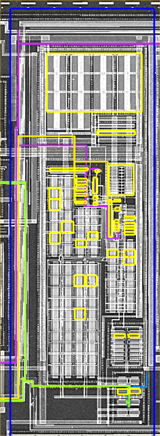
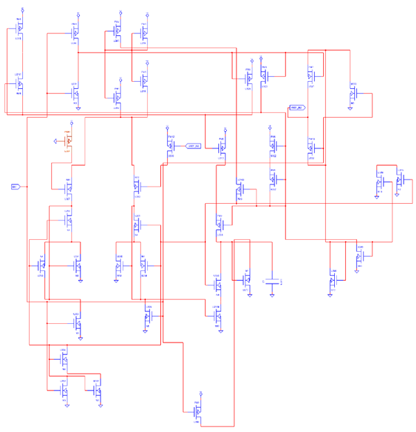
Invasive attacks on a security IC consist of direct die-level circuit probing, modification, deprocessing, and reverse engineering, again with the objective of compromising the solution by obtaining keys, disabling functionality, or completely reverse engineering the design to a netlist for reproduction. The skill set and required tools are more complex than in the non-invasive scenarios, but they do exist and are commonly used to attack the security ICs that protect high-value assets. For example, Figure 1 and Figure 2 are examples of the output from tools that can be used with an invasive attack to first image a portion of an IC and then extract the netlist and schematics from the imaging. An attacker would repeat this process for the entire IC with the ultimate goal of gaining some insight to launch a sub-circuit attack or producing a database to replicate the IC.
Like the non-invasive situation, there are circuit solutions available to combat invasive attacks. One example consists of top-level die shields that are actively monitored for a tamper event and combined with detection circuitry that takes defensive counteraction. However, the skills and equipment of attackers employing invasive techniques quickly evolve and have historically been a challenge to decisively defeat.
How PUF Technology Counters Invasive Attacks
Physically unclonable function (PUF) technology has emerged to provide strong protection against invasive threats. PUF is derived from the complex and variable physical/electrical properties of ICs. Because PUF depends on random physical factors (unpredictable and uncontrollable) that exist natively and/or are incidentally introduced during a manufacturing process, it is virtually impossible to duplicate or clone. PUF technology natively generates a digital fingerprint for its associated security IC, which can be utilized as a unique key/secret to support cryptographic algorithms and services including encryption/decryption, authentication, and digital signature.
A PUF implementation from Maxim Integrated operates on the naturally occurring random variation and mismatch of the analog characteristics of fundamental semiconductor MOSFET devices. This randomness originates from factors such as oxide variation, device-to-device mismatch in threshold voltage, and interconnect impedances. Similarly, the wafer manufacturing process introduces randomness through imperfect or non-uniform deposition and etching steps. Paradoxically, semiconductor device parameter variation is normally a challenge that IC designers face during development and is the fundamental basis that is exploited for Maxim’s PUF design.
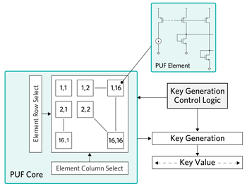
Figure 3 is a simplified block diagram of the Maxim PUF architecture with an example key size of 128 bits. Shown within the PUF core block is a 16×16 array of 256 PUF elements, each of which is an analog structure. Through factory conditioning, these 256 elements are combined into 128 pairs. When comparing structure to structure, random I/V characteristics exist due to the previously described parameters and are utilized to generate binary 1/0 values through a precision circuit-level comparison of each element within a pair. For example, elements {2,1} and {14,16} could constitute a pair, and the I/V characteristics of each are compared to derive a bit value. This is repeated with each of the 128 pairs to produce a 128-bit PUF key output for the example key size. For larger key size requirements, the number of PUF elements is simply scaled.
For invasive attacks, any probing or attempted analog measurement of a PUF element causes the sensitive analog electrical characteristic to change due to factors including capacitive/inductive/resistive loading. This is why it is impossible to extract any key data through invasive measurements. Also, because of the statistical nature of imperfect manufacturing techniques, there is no known method to discern any key information from inspection methods. Similarly, even knowledge of the PUF element paring does not reveal any information about the key value that can be ultimately derived from the analog characteristics of the PUF element structures. Finally, the PUF key value only exists digitally when a cryptographic operation is performed; thereafter, it is instantaneously erased. These PUF attributes together result in a solution that is highly immune to invasive attacks.
PUF Reliability and Cryptographic Quality
From a cryptographic perspective, reliability and randomness are critical characteristics that a PUF solution must exhibit. For use as a cryptographic key, or root thereof, the PUF output must have 100% reliability, meaning PUF-derived key bit values must be repeatable over time and all operating conditions. For semiconductor devices, this evaluation is performed using JEDEC-defined, industry-proven methods of reliability study. This includes selecting and subjecting a statistically significant sample set of devices to environmental and operational stress conditions that enable evaluation of lifetime reliability performance. These stresses include high-temperature operating life (HTOL), temperature cycling, packaging and solder reflow influences, voltage and temperature drift, and highly accelerated temperature/humidity stress testing (HAST). Performing a reliability qualification study using these proven methods results in a statistical assessment of how a design performs over the life of its use in a system. For example, consider that a system end product has a design life of 10 years and operates within -40°C to +85°C environments with power sources that can fluctuate by ±10%.
Equally critical with a PUF solution is the requirement for high-performance cryptographic quality, with a critcal property being randomness. Low-quality randomness can create a cryptographic attack vulnerability through predictability weakness. Statistical test suites, including the NIST SP 800-22, provide an industry-proven means to measure the randomness of the PUF output. Evaluation against the test suite provides several metrics, which determine whether the PUF output is consistent with a random sequence. To be statistically significant, these tools require large data sets for the analysis (e.g., 20-kbit sequences). Therefore, the output from a large set of PUF instances is required and used for the assessment.
Reliability Studies on PUF
A lifetime reliability analysis of Maxim’s PUF yielded results that demonstrated its capabilities. Fundamentally, the reliability study produced data to understand the PUF elements, such as the shift from aging, temperature/voltage drift, IC packaging, and PCB assembly. Relative to the time-zero characteristics of two PUF paired elements, the paired elements after the reliability study are shown to consume approximately 7% of the total margin available to maintain the stability of the output binary value. The final output from the analysis is a PUF key error rate (KER) of ≤ 5ppb, where KER is defined as the probability that 1 bit within the total key size produced by the PUF (e.g., 256 bits) can flip over the life of the product.
A randomness assessment of the PUF relied on performance to the NIST standard SP 800-22 monobit, poker, runs test, and long run test. These test suites evaluate whether output data is consistent with a random sequence. Assessment results for each of the four tests validate excellent performance with respect to randomness.
To evaluate the immunity to invasive attacks and reverse engineering, the Maxim PUF solution was evaluated by a leading US-based company that specializes in die level security assessments and IC reverse-engineering expertise. In the given assessment timeframe, the PUF operation was not compromised, and there was a qualitative conclusion that the solution is “highly effective and resistant against physical Reverse Engineering attacks.”
PUF Use Cases
There are numerous ways PUF technology can be used for cryptographic operations within security ICs, some examples:.
In Figure 4, to secure all stored data on a security IC, the PUF-derived key is used to encrypt/decrypt data as needed using an algorithm such as AES. If an invasive attack gains access to any nonvolatile memory (NVM) data, that data is useless because it is encrypted and the attacker is not able to obtain the PUF-based decryption key. In this example the encryption/decryption of data is done exclusively on-chip as needed. PUF key encrypted data is not transmitted from the IC.
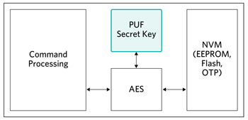
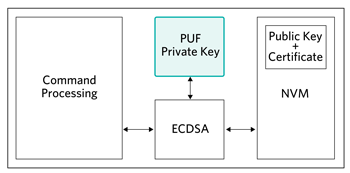
Figure 5 shows the use of PUF as the unique private key for ECDSA signing operations. For this case the device would compute its own corresponding public key from the PUF private key and a certificate would be installed in NVM by a certificate authority prior to end-use deployment.
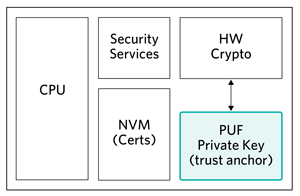
In Figure 6, the PUF private key is the root private key for the security IC and is used in conjunction with the end system to establish a “root of trust” with the security IC for subsequent services.
Maxim’s Commercial PUF-Based Security ICs
Maxim currently offers two ChipDNA PUF-based security ICs: the DS28E38 with asymmetric ECDSA-based authentication and the DS28E50 with symmetric SHA3-based authentication.
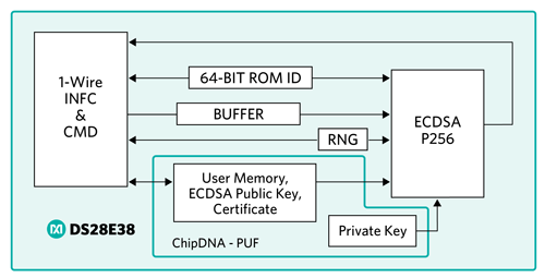
The DS28E38 is an ECDSA authenticator that utilizes the company’s ChipDNA PUF output as key content to cryptographically secure all device-stored data. Optionally, under user control, ChipDNA technology is used as the private key for ECDSA signing operations. The device provides a core set of cryptographic tools derived from integrated blocks including the asymmetric (ECC-P256) hardware engine, a FIPS/NIST-compliant true random number generator (TRNG), 2Kb of secured EEPROM, a decrement-only counter, and a unique 64-bit ROM identification number (ROM ID). The ECC public/private key capabilities operate from the NIST-defined P-256 curve to provide a FIPS 186-compliant ECDSA signature-generation function. A block diagram of the DS28E38 is shown in Figure 7.
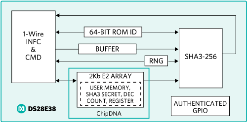
The DS28E50 is a SHA3 authenticator which, like the DS28E38, utilizes the PUF output as an encryption/decryption key to secure all device-stored data. The device provides FIPS-202 compliant bi-directional SHA3-256 based authentication, a FIPS/NIST-compliant TRNG, 2Kb of secured EEPROM, a decrement-only counter, a secure GPIO, and unique 64-bit ROMID. A block diagram of the DS28E50 is shown in Figure 8.
Summary
Cryptography protects the electronic assets inside embedded systems. By using security ICs with cryptographic functions in their embedded designs, designers benefit from strong design protection without having to be cryptography experts. However, the security ICs themselves can become the targets of attack by increasingly sophisticated cybercriminals. Based on its inherent qualities, PUF technology is highly immune to reverse-engineering methods, providing a decisive countermeasure to invasive attacks.
Courtesy: www.maximintegrated.com