The quantum revolution that is poised to transform computing and communications is all worked out, in theory. The practicalities, however, are proving stubborn: manipulating matter and energy at the incredibly small scales required is no easy feat and often requires exotic materials and temperatures near absolute zero.
A compound called hexagonal boron nitride (hBN) may save the day. According to a pair of Australian physicists writing in Science, it is about to make many quantum dreams a reality.
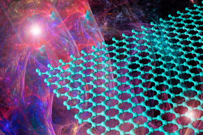
The material has a honeycomb crystalline structure, like graphite, and can be created in thin sheets comprising just a single layer of atoms. What’s more, it can be made to emit single photons on demand without any fancy refrigeration.
That property was discovered in 2016, by a team of researchers at the University of Technology Sydney in Australia. The two authors of this new Science article, Igor Aharonovich and Milos Toth, were part of that team.
Many proposed quantum devices – computers, communicators, and sensors – rely on having a reliable and easy way to manipulate single photons. A contraption that can do this (a so-called single-photon emitter, or SPE) could form the building block of integrated circuits, or use quantum effects for secure communication, or even – closer to home, though of less scientific interest – power televisions and displays with more vivid and realistic colour.
There have been two main ideas for how to build SPEs. The first is quantum dots, which are tiny particles that can be engineered to emit photons of a given frequency on demand. While these are an area of very active research, at present most only function at extremely cold temperature.
The second is “colour centres”, which are tiny impurities in solid materials such as diamond that can emit or trap photons of a specific frequency (or colour). The studies of these took off in 2015 with the creation of two-dimensional colour centre SPEs. The atomic thinness allows easy transmission and absorption of photons, but these again only worked at very low temperatures.
Enter hBN, which does away with the need for cryogenics and opens the way to much wider use of the technology.
“Scientific applications are here already,” says Aharonovich. “It’s so far the brightest single photon source. Many people use it for calibration of their setups, and confocal microscope alignment.”
Commercial applications may only be 3–5 years away, he adds, if everything “works as we think it should”. Even so, it won’t all be plain sailing. Making single-layer hBN itself in any large quantity “will require dramatic advances in fabrication methods”.


