


 voltage controlled oscillator (VCO). An efficient boost converter provides this voltage, and the circuit operates on a single 5 V)
Circuit Function & Benefits
The high performance PLL synthesizer circuit in Figure 1 requires 28 V for the tuning voltage of an octave range (1 GHz to 2 GHz) voltage controlled oscillator (VCO). An efficient boost converter provides this voltage, and the circuit operates on a single 5 V supply with no measurable degradation on the phase noise due to the dc-to-dc boost converter.


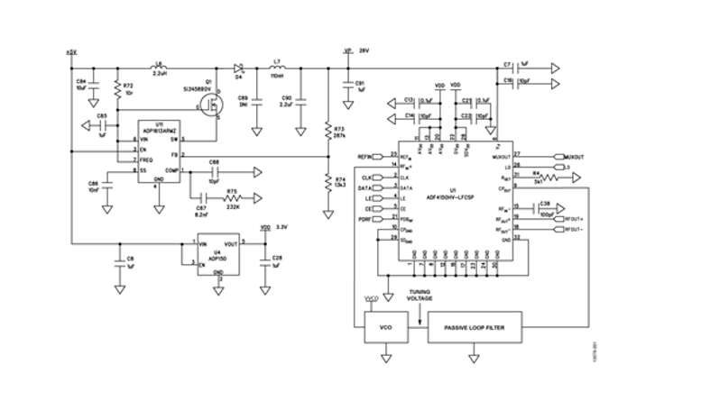 Figure 1. Boost Converter Used for the High Voltage Charge Pump Supply of the ADF4150HV (Simplified Schematic: All Connections Not Shown)
The circuit is optimized for PLLs that use octave range VCOs to provide a wide range of output frequencies. This type of VCO requires a high tuning voltage that may not be available in most systems that operate on relatively low supply voltages.
For example, the VCO in the circuit (Synergy DCYS100200-12) covers the 1 GHz to 2 GHz frequency band; however, to use the full octave range available, a tuning voltage of 0 V to 28 V is required.
There are two ways to supply this tuning voltage. The traditional technique uses an active loop filter with the amplifiers supplied by the high voltage supply. The optimum technique, however, uses a high voltage PLL synthesizer, such as the ADF4150HV, where the PLL provides the tuning voltage without the need for an active loop filter.
Although both solutions require a high voltage supply, the ADF4150HV eliminates the need for an active loop filter, which not only reduces component count and costs, but also reduces the distortion and phase noise associated with the amplifiers in the active filter. The high voltage supply is connected to the VP pin of the ADF4150HV charge pump, and any ripple on the supply is isolated from the VCO input by the passive loop filter.
The decreased sensitivity to distortion and ripple allows an efficient dc-to-dc boost converter to generate the 28 V supply for the charge pump supply pin (VP) of the ADF4150HV from a 5 V supply. See “Power Management Design for PLLs,” Analog Dialogue, 45-09, for a complete discussion on powering PLLs.
Figure 1 shows an industry-leading solution using the ADF4150HV and the ADP1613 boost converter. Total board area for the boost regulator is only 43 mm2, and the ADP1613 is available in an 8-lead MSOP package.
Circuit Description
The circuit shown in Figure 1 uses the ADF4150HV, a high voltage fractional-N PLL IC, and the ADP1613, a step-up switching converter.
The circuit is driven from a single 5 V supply connected to the input of the ADP1613. The ADP150, an ultralow noise LDO provides the 3.3 V VDD voltage connected to the AVDD, DVDD, and SDVDD pins of the ADF4150HV.
Note that all the AVDD pins of the ADF4150HV share common decoupling, the supply for the digital block (DVDD and SDVDD) requires a separate set of decoupling capacitors.
The ADP1613 is a dc-to-dc boost converter with an integrated power switch and an allowable output voltage of up to 20 V. Higher voltages are possible using additional external components. The pin selectable switching frequency of 650 kHz or 1.3 MHz allow excellent transient response and easy noise filtering.
The ADIsimPower design tool provides an easy way for designers to determine the appropriate components based on input and output requirements. The design of the ADP1613 circuit shown in Figure 1 uses the ADP161x downloadable boost designer tool. The inputs to the tool are the highest efficiency option together with the advanced settings of VOUT ripple = 0.2%, VOUT step error = 1%, and the noise filter option. The input voltage is set to VINMIN = 4.5 V, VINMAX = 5.5 V, the output voltage = 28 V, the output current = 40 mA, and the ambient temperature = 25°C. The design file is included as part of the CN-0228 Design Support package at www.analog.com/CN0228-DesignSupport.
The ADIsimPower design file includes the bill of material, detailed schematic, bode plots, efficiency plots, transient response, and a suggested board layout.
The ADF4150HV is a 3.0 GHz, fractional-N or integer-N frequency synthesizer with an integrated high voltage charge pump. The ADP1613 provides the 28 V required for the high voltage, integrated charge pump supply of the ADF4150HV.
The synthesizer directly drives the external wideband VCOs, thereby eliminating the need for operational amplifiers to achieve higher tuning voltages. This simplifies design and reduces cost, while improving phase noise, in contrast to the active filter topologies, which tend to degrade phase noise compared to the passive filter topologies.
When paired with an octave tuning range VCO, the ADF4150HV provides an ultra-wideband PLL function using the on-board RF dividers. With an octave tuning range at the fundamental frequency, the RF dividers provide full continuous frequency coverage down to much lower frequencies. For example, using a 1 GHz to 2 GHz octave range VCO (such as the Synergy DCYS100200-12), the user can obtain continuous output frequencies from 62.5 MHz to 2 GHz at the ADF4150HV RF outputs, as shown in Figure 2. A broadband output match is achieved using a 27 nH inductor in parallel with a 50 Ω resistor (for more information, see the ADF4150HV data sheet). With such a wide output range, the same PLL hardware design can generate different frequencies for a number of different hardware platforms in the system.
 Figure 2. Ultrawideband PLL Using the ADF4150HV and an Octave Range VCO (Simplified Schematic: All Connections and Decoupling Not Shown)
 Figure 3. Frequency Spectrum for a 1.5 GHz Output
Common Variations
The high voltage supply in this circuit is useful for microwave VCOs that need a wide tuning voltage range.
The 3.3 V supply can be derived from a 5 V supply using the ADP150 or ADM7150 low noise LDOs. Many microwave VCOs can operate on the 5 V supply.
When designing with different VCOs, design a relevant loop filter to ensure that the phase-locked loop works well. The ADIsimPLL design tool provides an easy way for designers to determine the appropriate components based on VCO sensitivity (KV), PFD frequency, channel spacing, and other requirements.
Alternate dc-to-dc switching converters can be used, however, for PLL synthesizers charge pump supply, it is advisable to choose a boost converter with a high switching frequency (more than 1 MHz). The loop filter of the phase-locked loop can reduce/ suppress the spurs caused by the switching frequency of the boost converter.
Circuit Evaluation & Test
The circuit shown in Figure 1 is part of the EV-ADF4150HVEB2Z evaluation board. A complete schematic, layout, and bill of materials for the evaluation board can be found at www.analog.com/CN0228-DesignSupport.
The Synergy DCYS100200-12 VCO used on the evaluation board requires a clean 12 V supply, which is provided from the output of an ADP7104 adjustable low noise LDO. However, to achieve good output voltage accuracy, the input voltage of the adjustable LDO must be at least 1 V higher than the output voltage, thus the supply of the board is set to the closest standard supply value above the necessary minimum (13 V), that is, to 15 V.
The input voltage to the ADP1613 dc-to-dc boost converter can accept 5.5 V maximum; therefore, on the evaluation board, it is limited to 5.1 V. This is achieved with a 5.1 V Zener diode biased with a 300 Ω resistor connected to the 15 V supply. The Zener diode then drives the input to the ADP1613.
The 28 V supply on the VP pin of ADF4150HV is generated using the circuit shown in Figure 1. Results measured with the EV-ADF4150HVEB2Z evaluation board using the ADP1613 boost converter are shown in Figure 3. The evaluation software, ADF4150HV family software, controls all the features available on the ADF4150HV evaluation boards. A description of the EV-ADF4150HVEB2Z board is available in the UG-483 User Guide.
For more information, visit: www.analog.com