

 DRAM structure and (b) Cross section view of saddle fin along with key specifications of the saddle fin profile.")
In the world of advanced semiconductor fabrication, creating precise device profiles (edge shapes) is an important step in achieving targeted on-chip electrical performance. For example, saddle fin profiles in a DRAM memory device must be precisely fabricated during process development in order to avoid memory performance issues. Saddle Fins were introduced in DRAM devices to increase channel length, prevent short channel effects, and increase data retention times.
Critical process equipment settings like etch selectivity or the gas ratio of the etch process, can significantly impact the shape of fabricated saddle fin profiles. These process and profile changes have significant impact on DRAM device performance. It can be challenging to explore all possible saddle fin profile combinations using traditional silicon testing, since wafer-based testing is time-consuming and expensive. To address this issue, virtual fabrication software (SEMulator3D) can be used to test different saddle fin profile shapes without the time and cost of wafer-based development.


In this article we review an example of using virtual fabrication for DRAM saddle fin profile development. We also assess DRAM device performance under different saddle fin profile conditions. This methodology can be used to guide process and integration teams in the development of process recipes and specifications for DRAM devices.
The Challenge of Exploring Different Profiles
Imagine you are a DRAM process engineer, and have received nominal process conditions, device specifications, and a target saddle fin profile for a new DRAM design. You want to explore some different process options and saddle fin profiles to improve the performance of your DRAM device. What should you do? This is a common situation for integration and process engineers during the early R&D stages of DRAM process development.
Traditional methods of exploring saddle fin profiles are difficult and sometimes impractical. These methods involve the creation of a series of unique saddle fin profiles on silicon wafers. The process is time-consuming, expensive, and in many cases impractical, due to the large number of scenarios that must be tested.
One solution to these challenges is to use virtual fabrication. SEMulator3D allows us to create and analyze saddle fin profiles within a virtual environment and to subsequently extract and compare device characteristics of these different profiles. The strength of this approach is its ability to accurately simulate the real-world performance of these devices, but to do so faster and less-expensively than using wafer-based testing.
Let’s dive into the methodology behind our approach.
Creating Saddle Fin Profiles in a Virtual Environment
First, we input the design data and process flow (or process steps) for our device in SEMulator3D. The software can then generate a “virtual” 3D DRAM structure and provide a visualization of saddle fin profiles (Figure 1). In Figure 1(a), a full 3D DRAM structure including the entire simulation domain appears. To enable detailed device study, we cropped a small portion of the simulation domain from this large 3D area. In Figure 1(b), we extracted a cross sectional view of the saddle fin structure, which can be modified by varying a set of multi-etch steps in the process model. The section of the saddle fin we want to modify is identified as the “AA” (active area). We can finely tune the etch taper angle, AA/fin CD, fin height, taper angle, and additional nominal device parameters to modify the AA profile.
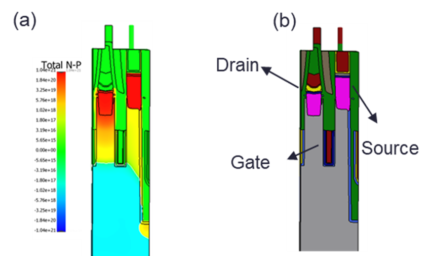
Using the structures, we built in SEMulator3D, we next assign dopants and ports to the simulated structure and perform electrical performance evaluation. Accurately assigning dopant species and defining dopant concentrations within the structure is critical to ensuring the accuracy of our simulation. In Figure 2(a), we display a dopant concentration distribution generated in SEMulator3D.
Ports are contact points in the model, which are used to apply or extract electrical signals during a device study. Proper assignment of the ports is very important. Figure 2(b) provides an example of port assignment in our test DRAM structure. By accurately assigning the ports and dopants, we can extract the device’s electrical characteristics under different process scenarios.
Manufacturability Validation
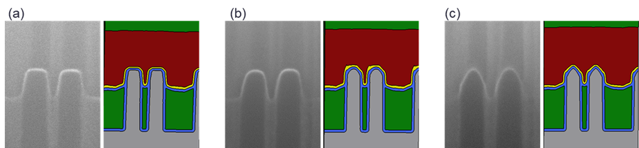
It is important to ensure that our simulation models match real world results. We can validate our model against cross-sectional images (SEM or TEM images) from an actual fabricated device. To ensure our simulated device matches the behavior of an actual manufactured chip, we can create real silicon test wafers containing DRAM structures with different saddle fin profiles.
To study different saddle fin profiles, we use different etch recipes on an etch machine to vary the DRAM wordline etch step. This allows us to create specific saddle fin profiles in silicon that can be compared to our simulated profiles. A process engineer can change etch recipes and easily create silicon-based etch profiles that match simulated cross section images, as shown in Figure 3.
In this case, the engineer created a nominal (Process of Record) profile, a “round” profile (with a rounded top), and a triangular shaped profile (with a triangular top). This wafer-based data is not only used to test electrical performance of the DRAM under different saddle fin profile conditions, but can also be fed back into the virtual model to calibrate the model and ensure that it is accurate during future use.
Device Simulation and Validation
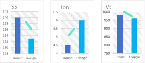
In the final stage of our study, we review the electrical simulation results for different saddle fin profile shapes. Figure 4 displays simulated electrical performance results for the round profile and triangular saddle fin profile. For each of the two profiles, the value of the transistor Subthreshold Swing (SS), On Current (Ion), and Threshold Voltage (Vt) are displayed, with the differences shown. Process integration engineers can use this type of simulation to compare device performance using different process approaches. The same electrical performance differences (trend) were seen on actual fabricated devices, validating the accuracy and reliability of our simulation approach.
Conclusion
SEMulator3D provides numerous benefits for the semiconductor manufacturing industry. It allows process integration teams to understand device performance under different process scenarios and lets them easily explore new processes and architectural opportunities.
In this article, we reviewed an example of how virtual fabrication can be used to assess DRAM device performance under different saddle fin profile conditions. Figure 5 displays a summary of the virtual fabrication process and how we used it to understand, optimize, and validate different process scenarios.
Virtual fabrication can be used to guide process and integration teams in the development of process recipes and specifications for any new memory or logic device and to do so at greater speed and lower cost than silicon-based experimentation.