


1 Description
The TIDA-00951 design provides a reference solution for a 2-kW isolated bidirectional DC-DC converter capable of power transfer between a 400-V DC bus and a 12- to 14-cell Lithium battery pack for use in UPS, battery backup and power storage applications.


This TI Design works as a >93% efficient, current fed, active clamped boost converter with ZVS in the backup mode and voltage fed full-bridge batter charger with >93% efficiency in the charging mode. This TI Design has built-in protection for DC bus overcurrent and overvoltage and battery overcurrent.
2 Features
- Digitally Controlled Isolated Bidirectional DC-DC Converter
- Operates as Active Clamped Full Bridge Boost Converter With ZVS For All Low-Voltage Switches at High Loads
- Operates as Active Clamped Voltage Fed Buck Converter With Synchronous Rectification to Improve Efficiency When Charging Battery
- Wide Operating Range From 36- to 60-V Battery and 300- to 400-V DC Bus
- Cost Optimized Design Using 100-V FET on LowVoltage Side, Eliminates Requirement for Paralleling Multiple FETs up to 2 kW
- Built-in Cold Start Procedure and Fast Mode Transfer (< 100 µS) From Battery Charger to Backup Power Supply
- Onboard Isolated Communication Interface for CAN, I2 C, and RS-485
3 Applications
- Server PSUs and Telecom Rectifiers
- Uninterruptible Power Supplies ( UPS )
- Industrial Power Supplies
- Battery Chargers
- Energy Storage Systems
 4 System Description
Description
Most backup power equipment such as DC inverters, home inverters, industrial DC-UPS, and energy storage banks require an exchange of power from the battery to the load and vice versa. Typical power system distribution architecture with battery backup is shown in Figure 1:
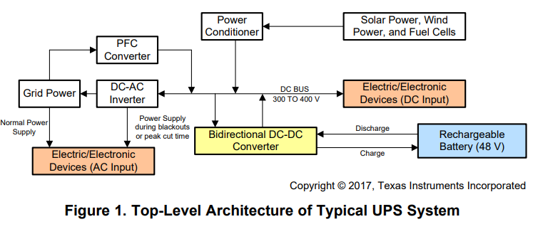 Figure 1. Top-level Architecture of Typical UPS System
During normal operation, the main DC bus is regulated between 300 and 400 V through the grid source of a building, factory, or house. Alternatively, the DC bus can be powered through a renewable energy source such as solar power generation or wind power generation, which is conditioned through a power conditioner to feed the DC bus. The battery acts as an energy storage unit, and it can be charged either through the grid or an external renewable energy source.
Conventionally, charging a battery through a DC bus and discharging the battery during power blackouts are implemented with two unidirectional converters, each processing the power in one direction. With a growing emphasis on compact and efficient power systems, there is increasing interest in using bidirectional converters, especially in DC inverters, home inverters, and energy storage banks. A bidirectional DC-DC converter, capable of bilateral power flow, provides the functionality of two unidirectional converters in a single converter unit.
The TIDA-00951 design is an isolated bidirectional DC-DC converter designed to exchange the power between a 300- to 400-V DC Bus and 48-V battery banks. The design has a full-bridge power stage on the high-voltage (HV) side, which is isolated from a current-fed full-bridge stage on the low-voltage (LV) side. During the presence of the DC bus (normal conditions), the design operates in buck mode and charges the battery with constant current until the battery voltage is in regulated limits. During blackouts, the design operates as the current-fed full-bridge converter to boost the power from a 48-V battery (36- to 60-V input) to the 380-V DC bus and supports the load with backup.
System Description
The transition or change over time from the charge to backup mode is very critical for ensuring continuity of power to the loads. The TIDA-00951 has transition time of less than 100 µs, which reduces the amount of bulk capacitance needed for the system to provide power during the transition time.
This TI Design operates at peak efficiency of 93% in buck mode (as charger) and 94% in boost mode (during discharge). The high discharge efficiency provides a high run time from the battery. Operating at a high switching frequency of 100 kHz, the design has a compact form factor of 185 mm × 170 mm for the power level of 2 kW.
The TIDA-00951 design is optimized for component count, cost, and performance. Various parameters of the design like regulation, efficiency, output ripple, transition time, startup, and switching stress across the devices were tested and documented in the following sections.
Description
4.1 Key System Specifications
Table 1. Key System Specifications
| PARAMETER | TEST CONDITIONS | MIN | NOM | MAX | UNIT |
| BACKUP SUPPLY MODE | |||||
| INPUT CONDITIONS | |||||
| Input battery voltage (VBAT) | — | 36 | 44.4 | 60 | V |
| Input battery current (IBAT_MAX) | — | — | — | 60 | A |
| OUTPUT CONDITIONS | |||||
| Output bus voltage (VBUS) | — | 300 | 380.0 | 400 | V |
| Output bus current (IBUS_ MAX) | VBAT > 40 V | — | — | 5 | A |
| Line regulation | — | — | 1 | % | |
| Load regulation | 10% to 100% load | — | — | 1 | % |
| Output voltage ripple | — | — | — | — | — |
| Input voltage ripple | — | — | — | — | — |
| Average efficiency | 20% to 100% | — | — | — | % |
| Full load efficiency | — | — | — | — | % |
| BATTERY CHARGER | |||||
| INPUT CONDITIONS | |||||
| Input bus voltage (VBUS) | — | 300 | 380.0 | 400 | V |
| Input bus current (IBUS_ MAX) | — | — | — | 60 | A |
| OUTPUT CONDITIONS | |||||
| Output battery voltage (VBAT) | — | 36 | 44.4 | 60 | V |
| Output battery current (IBAT) | — | — | — | 16 | A |
| SYSTEM SPECIFICATIONS | |||||
| Operating ambient | — | –10 | 25 | 55 | °C |
| Board size | Length × Width × Height | 185 × 173 × 8 | mm | ||
5 System Overview
5.1 Block Diagram
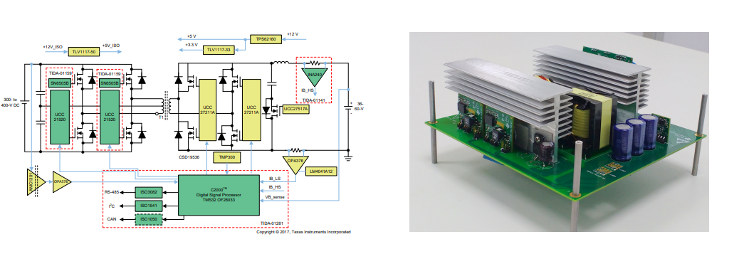
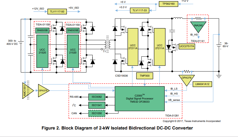
Figure 2 shows the high-level block diagram of the TIDA-00951. The DC-DC converter is made of a current-fed full-bridge converter on the battery side and a full-bridge on the 380-V bus side. The control of the system is through the C2000 present on the TIDA-01281 control card. The TIDA-01159 isolated gate driver card is used to drive the full bridge on the 380-V bus side. High-side inductor current sensing is performed using the TIDA-01141 board.
5.2 System Design Theory
The isolated bidirectional DC-DC converter has two major modes of operation. When it is working as a backup power supply, it operates as an active clamped current-fed boost converter transferring power from the battery to the 380-V DC bus. When operating as a battery charger, the DC-DC converter works as a buck converter transferring power from the 380-V DC bus to the battery.
Apart from the two major modes, there is an additional mode for the cold starting the system. This mode is used to start up the TIDA-00951 in case the HV DC bus is completely discharged before board start-up.
The working of the isolated bidirectional DC-DC converter design is detailed in the following sections.
5.2.1 Boost Mode
5.2.1.1 Topology Description
When working in boost mode, the system needs to boost an input voltage between 36 to 60 V to a 380- V DC output. There are multiple topologies that can be considered for this TI Design.
Broadly speaking, the possible topologies can be classified into voltage- or current-fed topologies have an input inductor, which is connected to the power stage. However, a voltage-fed converter connects the input filter capacitor to the power stage. The presence of this input inductor gives the following benefits:
- Boosted voltage reduces the stress in the transformer and better utilization
- Avoids flux imbalance issues in the power stage
- Lower stress on the input filter capacitors due to reduction in the current ripple due to the input inductor
The TIDA-00951 works as an active clamped current-fed full-bridge converter in boost mode. Although there are several advantages in using a current-fed converter, one primary disadvantage is the huge spike in the current-fed converter at MOSFET turnoff. This turnoff requires some form of snubbing using either an active or passive snubber.
In the TIDA-00951 design, an active clamp compromising of a capacitor and a MOSFET has been used to implement an active snubber. The advantage of this active clamp is that not only does it recover the leakage energy, but it also helps in achieving ZVS for the primary LV MOSFET at turnon, thereby reducing the switching losses.
When working as a battery charger, the TIDA-00951 works as a voltage-fed buck converter. It transfers power from the HV DC bus and charges the battery in constant-current/constant-voltage (CC/CV) mode with a current limit of 16 A.
The following two sections explain how the converter in the backup supply mode works.
5.2.1.2 Boost Mode Working: Active Clamp
power stage of the TIDA-00951 is shown in Figure 3.
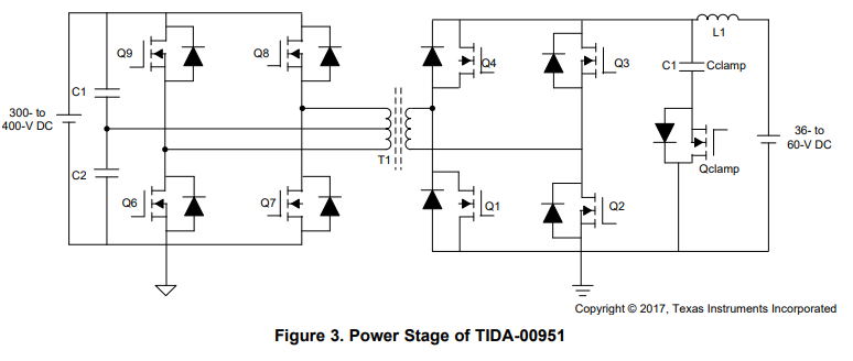 The switches Q1 to Q4 are the LV-side full-bridge MOSFET. The switches Q6 to Q9 form the HV-side fullbridge MOSFET. The capacitor Cclamp and switch Qclamp form the active clamp.
When the system works as a current-fed full bridge, transferring power from the battery to the DC bus, the active clamp stores the additional leakage energy when the MOSFET Q1 to Q4 turnoff, thereby limiting the turnoff spike on the MOSFET. Additionally, by controlling the switching of the MOSFET Q5, the primary LV MOSFET can be turned on in or close to 0 V, thereby reducing the turnon switching losses.
The modality of implementing this scheme is shown in Figure 4.
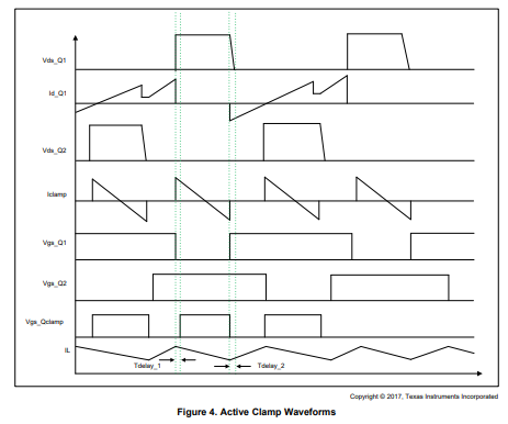 Figure 4. Active Clamp Waveforms
Take the switch pair Q1 and Q3 as an example to describe the working of the active clamp. When the switch pair Q1 to Q3 turn off, the current through FETs before turnoff get transferred and start flowing into the clamp capacitor and the body diode of Qclamp. Because the clamp current is flowing through the body diode of Qclamp, it can be turned on after a short time (Tdelay_1) in ZVS condition as shown in Figure 4.
Now, before the switch pair Q1 and Q3 is turned on again, the clamp FET Qclamp is turned off. Because the direction of the Iclamp has reversed and it is now flowing through the channel of the Qclamp, Iclamp instantly comes to zero.
Because the current through the leakage inductor cannot change instantly, a portion of the current flowing through the FET Qclamp, begins to flow through the body diode of FET Q1 and Q3. This begins to discharge the COSS of FETs Q1 and Q3 and causes ZVS to occur. After this, FETs Q1 and Q3 can be turned on under ZVS or close to ZVS condition, thereby reducing the turnon loss. The delay from the point of turnoff of the clamp FET Qclamp and turnon of Q1 and Q3 is marked as Tdelay_2 in Figure 4.
5.2.1.3 Boost Mode Working: Cold Start
Figure 5 shows the LV-side full-bridge converter along with the start-up clamp circuit.
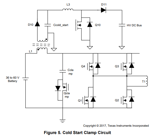 Figure 5. Cold Start Clamp Circuit
During the system start-up, if the HV DC bus is completely discharged. The TIDA-00951 starts up using an additional flyback winding present on the inductor L1. In this mode, the LV-side full bridge does not work as a current-fed converter but as a flyback converter. It works in this mode until the HV bus reaches 270-V DC and then the system switches over to working as a current-fed converter.
In Figure 5, the MOSFETs Q1, Q2, Q3, and Q4 form the LV-side full bridge. Qclamp and Cclamp form the active clamp. The flyback winding on the inductor L1 is used to temporarily charge a small capacitor, which is then boosted and fed to the HV DC bus output capacitors using the boost converter formed by Q10, D10, and L3.
Figure 6 shows the PWM waveforms of the LV MOSFETs Q1 to Q4, clamp MOSFET QClamp, and the boost MOSFET Q10. The figure also shows the current-fed inductor current waveform and the drain-to-source voltage waveform of the low-side bridge MOSFET.
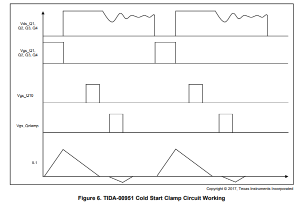 All the MOSFETs on the LV bridge are turned on simultaneously. This charges the current-fed inductor. When these MOSFETs are turned off, the current in the current-fed inductor is transferred to the flyback winding and energy is stored in the capacitor Ccold_start.
The boosted MOSFET Q10 is then turned on to charge the boost inductor L3. This energy is then transferred to the HV bus output capacitors.
5.2.1.4 Low-Side Current Sensing Circuit
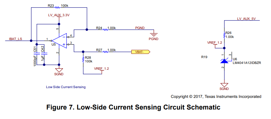
In the TIDA-00951, low-side current sensing is implemented to measure the battery current on the LV side using the OPA376.
Because the battery current is bidirectional in nature, the output of the OPA376 is 1.2 V by using the LM4041A12 shunt voltage reference. This is shown in Figure 7.
 Low Side Current Sensing SGND
The OPA376 difference amplifier measures the current across a 0.25-mΩ current sense resistor formed by the parallel combination of resistors of R20 and R29.
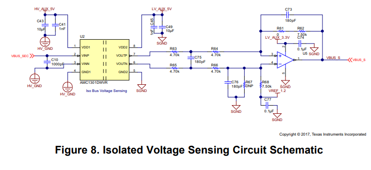
5.2.1.5 Isolated Voltage Sensing
The control electronics (TIDA-01281) on the TIDA-00951 board is referred to the LV battery-side ground. In order to sense the voltage across the isolated 400-V bus, an isolation amplifier circuit based around the AMC1301 isolated amplifier and OPA376 op amp is used.
The differential output of the AMC1301 is scaled and converted into a single-ended output for connecting directly to the MCU. Figure 8 shows this circuit.
Courtesy: www.ti.com