

 with high hole mobility, which allows reduced)
Using a new fabrication technique, NIMS has developed a diamond field-effect transistor (FET) with high hole mobility, which allows reduced conduction loss and higher operational speed. This new FET also exhibits normally-off behavior (i.e., electric current flow through the transistor ceases when no gate voltage is applied, a feature that makes electronic devices safer). These results may facilitate the development of low-loss power conversion and high-speed communications devices.
Diamond has excellent wide bandgap semiconductor properties: its bandgap is larger than those of silicon carbide and gallium nitride, which are already in practical use. Diamond therefore could potentially be used to create power electronics and communications devices capable of operating more energy efficiently at higher speeds, voltages, and temperatures. A number of R&D projects have previously been carried out with the aim of creating FETs using hydrogen-terminated diamonds (i.e., diamonds with their superficial carbon atoms covalently bonded with hydrogen atoms). However, these efforts have failed to fully exploit diamonds’ excellent wide bandgap semiconductor properties: the hole mobility (a measure of how quickly holes can move) of these diamond-integrated transistors was only 1–10% that of the diamonds before integration.


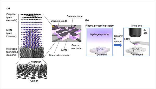
The NIMS research team succeeded in developing a high-performance FET by using hexagonal boron nitride (h-BN) as a gate insulator instead of conventionally used oxides (e.g., alumina), and by employing a new fabrication technique capable of preventing the surface of the hydrogen-terminated diamond from being exposed to air. At high hole densities, the hole mobility of this FET was five times that of conventional FETs with oxide gate insulators. FETs with high hole mobility can operate with lower electrical resistance, thereby reducing conduction loss, and can be used to develop higher speed and smaller electronic devices. The team also demonstrated the normally-off operation of the FET, an important feature for power electronics applications. The new fabrication technique enabled the removal of electron acceptors from the surface of the hydrogen-terminated diamond. This was the key to the team’s success in developing the high-performance FET, although these acceptors had generally been thought to be necessary for inducing electrical conductivity in hydrogen-terminated diamonds.
These results are new milestones in the development of efficient diamond transistors for high-performance power electronics and communications devices. The team hopes to further improve the physical properties of the diamond FET and to make it more suitable for practical use.