


Introduction
All the rage these days in the converter world is the GSPS ADC— otherwise known as an RF ADC. With such high sample rate converters available on the market this opens up the Nyquist by 10× as compared to five years ago. A lot has been discussed about the advantages of using RF ADCs and how to design with them and capture data at such high rates. Thank you JESD204x consortium. But one consideration seems to be forgotten about, the lowly dc signal.


The design of the input configuration, or front end, ahead of a high performance, analog-to-digital converter (ADC) is always critical to achieving the desired system performance. Typically the focus is capturing wideband frequencies, such as those greater than 1 GHz. However, in some applications, dc or near dc signals are also required and can be appreciated by the end user, as they too carry important information. Therefore, optimizing the overall front-end design to capture both dc and wideband signals requires a dc-coupled front end that leads all the way down to the high speed converter.
Because of the nature of the application, an active front-end design will need to be developed, as passive front ends and baluns used to couple the signals into the converter are inherently ac-coupled. In this article an overview on the importance of common-mode signals and how to properly level shift the amplifier front end will be presented in a real system solution example.
Common Mode: Overview
Many customer tech support questions still come in from customers when there is a lack of understanding of the common-mode parameter and how it relates to the devices. ADC data sheets specify a common-mode voltage requirement for the analog inputs. Not much detailed information is available on this subject, but the proper front-end bias must be maintained in order to achieve rated ADC’s performance at full scale.
ADCs with integrated buffers typically have an internally biased commonmode (CM) level of half the supply plus a diode drop (AVDD/2 + 0.7 V). No external circuitry is required to bias this circuit, but it must be maintained to properly use the converter. For unbuffered (switched capacitor input) converters, the common-mode bias is typically half the analog supply, or AVDD/2. This can be supplied externally in a variety of ways.
Some converters have a dedicated pin that allows the designer to provide bias through a couple of resistors tied to the analog inputs. Alternatively, the designer can connect the internal bias to a transformer’s center tap or can use a resistor divider off the analog supply (a resistor from each leg of the analog inputs to AVDD and ground). Check the manufacturer’s data sheet or applications support group before using the converter’s VREF pin, as many references are not equipped to supply a common-mode bias without an external buffer. It is tempting because the CM voltage you need is right there and handy, but be warned—don’t do it.
If the common-mode bias is not provided or maintained, the converter will have gain and offset errors that contribute to the overall measurement. The converter may clip early, or not at all, because the converter’s full scale cannot be reached. Common-mode bias is especially important when connecting an amplifier in front of the converter, especially if the application calls for dc coupling. Check the amplifier’s data sheet specifications to make sure the amplifier can meet the converter’s swing and common-mode supply requirements.
Converters have been pushing to smaller geometry processes and, therefore, lower supplies. With a 1.8 V supply, a 0.9 V common-mode voltage is required by the amplifier if dc coupling is required. Amplifiers with 3.3 V to 5 V supply voltages may not be able to maintain that low of a level, but newer low voltage amplifiers can, or the designer can use a split supply and use a negative rail on the VSS pins. However, when doing this, keep in mind other pins also may need to be connected to the negative rail. Consult the data sheet and/or the direct application support for the product to find out.
Common Mode: Defined
Let’s start with defining what a CM voltage is. Figure 1 shows how a converter sees differential and common-mode signals. A CM voltage is simply the center point around which the signals move—see Figure 1. You can also think of this as the new center point or zero code—an amplifier, CM is established on the outputs, usually through a VOCM pin or similar. Be careful though, these pins have certain current and voltage range requirements too. It might be best to review the amplifier data sheet and/or use a robust bias point that doesn’t load down any adjacent circuitry or reference point within your circuit. Don’t simply tap off a converter’s voltage reference pin (VREF), which is usually half the converter’s full scale. It may not be able to provide enough bias with good accuracy. It would be prudent to review the pin specifications on the converter’s data sheet as well. Usually something like a simple voltage divider with 1% resistor tolerances and/or a buffer driver will work to set this CM bias = properly for an amplifier.
In Table 1, a quick summary of how to connect the amplifier and converter per application is listed below, as well as some proper circuit examples shown in Figure 2.
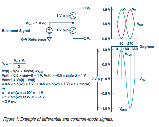
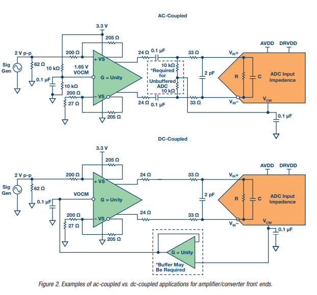
Table 1. Common-Mode Matrix
| Application | Amplifier | ADC | Notes |
| DC-Coupled | Set VOCM within limits specified on DS. Use voltage divider or buffer amp from ADC VREF/CML pin. | Does not provide CM bias. | Make sure both the amplifier and ADC CM bias are within range of each other.
Otherwise, a mismatch will cause errors. |
| AC-Coupled (with Unbuffered ADC) | Set VOCM within limits specified on
DS. Use voltage divider or some other stable bias point. |
Sets VIN CM bias to AVDD/2.
Use voltage divider or CML pin to provide CM bias. |
Place ac coupling caps on output of amplifier. |
| AC-Coupled (with Buffered ADC) | Set VOCM within limits specified on
DS. Use voltage divider or some other stable bias point. |
Does not provide CM bias. VIN pins are self biased to AVDD/2 + 0.7. | Place ac coupling caps on output of amplifier. |
Common Mode: Broken
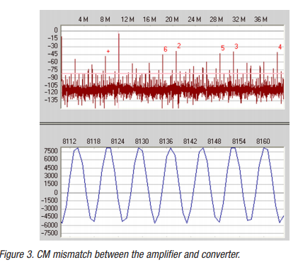
If the common-mode bias is not provided or maintained, then the converter will have gain and offset errors that degrade to the overall measurement being acquired. Simply put—the converter output will look like Figure 3 or some variation of it. The output spectrum will take on the form of looking like an overloaded full-scale input. This means the zero point of the converter is off center and not optimum. The designer may find that the converter will clip early or not reach the full scale of the converter. Recently this problem has gotten worse since converters are using 1.8 V supplies and lower.
This means the CM bias for the analog input is 0.9 V or AVDD/2. Not all single-supply amplifiers can support such a low commonmode voltage while maintaining relatively good performance. However, some new amplifiers have accommodated this and are out on the market today. Therefore, it would be prudent to review which amplifiers can be used in your new design. Not just any old amplifier will work because the headroom may become very constrained and the internal transistors start to cave in. If a dual supply is used with an amplifier, there should be sufficient headroom in most cases in order to achieve the proper CM bias. The downside is an extra supply—a negative supply that maybe nonstandard, which means more parts and more money. Simple inverter circuits will work to help with this.
 Putting It All Together
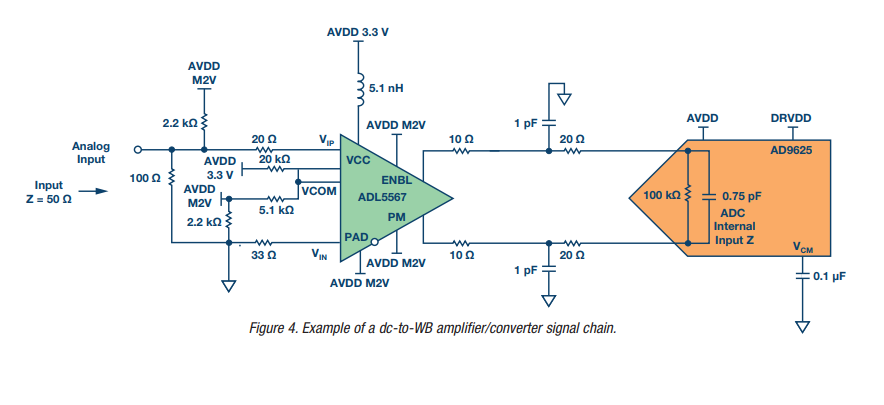
Now that common mode and dc coupling is understood, we can start putting together a signal solution. For example, the ADL5567, which is a dual differential amplifier with 20 dB of gain. It has 4.8 GHz of bandwidth and is suitable for interfacing with GSPS ADCs, like the AD9625 a 12-bit, 2.5 GSPS converter with a JESD204B 8-lane interface. Figure 4 shows the overall block diagram of the setup.
In this configuration shown, the front-end interface is optimized for wideband sampling while preserving the dc signal content. Since the part is +5.5 V tolerant. The design used a split +3.3 V and −2 V AVDD supplies. This made the common-mode alignment simple between the output of the amplifier and inputs of the ADC, both of which needs to be +0.525 V on both AIN+ and AIN−. Also, notice that a couple of the amplifier pin functions that were ground-enabled (Vss) with just a single power supply are now forced to the −2 V supply (new Vss).
The CM voltage outputs are fairly straightforward but the understanding of the amplifier inputs’ common-mode needs can be a bit tricky. There are two things that need to be done here for the interface. First, the input CM voltage needs to be configured for 0 V. Otherwise, driving the amplifier with offset will let the outputs rail to one side. This would cause the performance issues seen in Figure 3 or worse—where poor ac performance would be seen from the amplifier and converter signal chain. To do this, each side of the amplifier’s input needs to allow for current to flow to the ground, or 2 V in this dc-coupled case. Therefore, a 2.2 kΩ resistor was added to each amplifier input to kill this offset current.
Here is how that works: the output of the amplifier is ~0.525 V and the input CM voltage to the amplifier is 0 V. With an internal feedback resistor of 500 Ω and roughly a 50 Ω input resistor, this looks like 550 Ω; or in our case we assume a 50 Ω source resistance in parallel with 100 Ω, this gives us 33 Ω. The additional 20 Ω in series then sums to 53 Ω. This is in series with the 500 Ω internal feedback resistor or a grand total of 553 Ω. Which means a 0.525 V resistor divider of 500 Ω and 53 Ω is developed. Which in turn, develops a current of 900 μA, (or 0.525/553). To shunt this away to ground or the new VSS or −2 V, a 2.2 kΩ resistor was added or −2 V/2.2 kΩ = 900 μA.
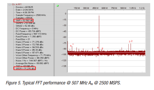
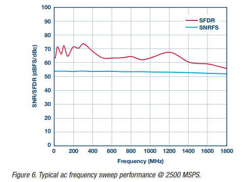
Second, the input is single ended and needs to be configured properly to hold best performance while maintaining a low even order distortion. Again, the effective 100 Ω in parallel with the 50 Ω source resistance yields a Thevenin equivalent to 33.33 Ω, as previously indicated. This, in turn, is typically reflected on both the VIN nodes to balance input of the device since it is being driven single ended. However, in order to improve even order distortion, 20 Ω on the VIN+ node was used to keep the distortion low across all wideband frequencies. This is done by using a specific midfrequency, ~500 MHz—or see Figure 5 as a test case. This can be tedious, as it is an iterative process. For calculations and equations in understand SE to DIFF conversion’s on amplifiers, see the ADA4932 data sheet. Typical ac performance sweeps over input frequencies of up to 2 GHz is shown for the signal chain design in Figure 6.
 It is also worth noting the addition of the 5.1 nH inductor in series with the power supplies’ positive rail input. This helps again to increase the even order linearity performance over frequency by capturing and recirculating these imbalanced currents internally in the amplifier.
Finally, the interface needs to be optimized for front-end BW between the amplifier and ADC. This is typically done in an iterative fashion as well. However, there are several notes to keep in mind on what sets certain values between the two ICs. The following list of rules can be applied in order to get the best BW out of the interface.
- First, select a kickback resistor (RKB), (Ω in this case), based on experience and/or the ADC data sheet recommendations, typically between 5 Ω and 36 Ω.
- Then, select the amplifier external series resistor (RA). Make RA <10 Ω if the amplifier differential output impedance is 100 Ω to 200 Ω. Make RA between 5 Ω and 36 Ω if the output impedance of the amplifier is 12 Ω or less. In this case, a 10 Ω series resistance was chosen with a differential output impedance of 10 Ω for the ADL5567.
- The total combination of resistors in series and parallel as seen by the amplifier’s outputs should be close to the characterized load (RL) of the amplifier. In this case, 160 Ω, or 2 RA + 2 RKB + RADC = 20 + 40 + 100, in the circuit of Figure 4. The ADL5567 was characterized with an RL of 200 Ω so expect some deviations in linearity performance if a design moves too far away from the characterized RL of the amplifier.
- Lastly, the internal ADC capacitance, CADC, adds to the shunt C shown after the 10 Ω series resistance to help with kickback from the internal ADC’s sampling network. This also offers soft low-pass filtering to diminish any wideband harmonics that fold back in-band.
For a more complete process in developing antialiasing filters between amplifiers and ADCs, see CN-0227 and CN-0238.
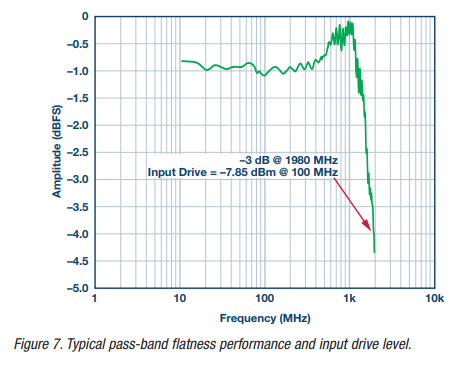
Using the criteria above a 2 GHz pass-band flatness response was developed in order to capture frequencies within the 1st and 2nd Nyquist zone, assuming 2.5 GSPS sampling. The input drive specification for this design ends up being −8 dBm or 252 mV p-p assuming a 50 Ω input impedance at 100 MHz reference. This is the input full-scale level at which the amplifier’s input requires for the converter to achieve full scale.
 Conclusion
Overlooking a converter’s common-mode input voltage specification can cause havoc in any dc-coupled design. If multiple stages are used, the common-mode levels must be kept the same throughout the signal chain to prevent the two components from fighting each other. One will usually win between any stage if not coupled correctly, producing bogus measurements.
For ac-coupled applications, use a coupling capacitor between the two stages to break the common-mode mismatches. This allows the design to optimize the bias of both the amplifier output and the ADC input, for example.
Otherwise, dual supplies or level shifting circuits will need to be involved in the system design, as described above in the dc-coupled design.
About the Author
Rob Reeder is a system application engineer with Analog Devices in the Aerospace and Defense Group in Greensboro, N.C., focusing on military and aerospace applications. He has published numerous articles on converter interfaces, converter testing, and analog signal chain design for a variety of applications. Formerly, Rob was an applications engineer for the high speed converter product line for eight years. His prior experience also includes test development and analog design engineer for the Multichip Products Group at ADI, designing analog signal chain modules for space, military, and high reliability applications for five years.
Article Courtesy: Analog Devices Inc.