


Introduction
When the wireless industry embarked on the creation of 5G, 2020 seemed so far away. Now we are quickly closing in on 2020 and this will most certainly be the 5G decade. Every day there are announcements in the press of new field trials and upcoming commercial 5G rollouts. It’s a very exciting time for the wireless industry. Currently, much of the industry 5G focus is on enhanced mobile broadband, driving toward higher and higher network capacity and throughput utilizing beamforming techniques in the mid band and high band spectrum. We are also beginning to see use cases emerge, such as industrial automation, that leverage the low latency features of the 5G network architecture.


It was only a few years ago that the industry was debating the feasibility of using the millimeter wave spectrum for mobile communications and framing the challenges that lay ahead for the radio designer. Much has transpired in a short time and the industry has progressed rapidly from initial prototypes to successful field trials and now we are on the verge of the first commercial 5G millimeter wave deployments. Many of the initial deployments will be for fixed or nomadic wireless applications, but we will also see truly mobile connectivity at millimeter wave frequencies in the not so distant future. The first standards are in place, technology is quickly evolving, and much learning has transpired around the deployment of millimeter wave systems. While we have made much progress, there remain many challenges ahead for the radio designer. Let’s examine some of these challenges for the RF designer in the remainder of this article.
This article is organized into three major topics. In the first section, we will discuss some of the leading use cases for millimeter wave communications and set the stage for the analysis that follows. In the second and third sections, we will delve into the architectures and technology for millimeter wave base station systems. In the second section, we will discuss technology for the beamformers and how the required transmit power influences the choice of technology for the system front end. While the beamformer receives much of the spotlight in the press, there is an equally important section of the radio that performs the conversion from bits to millimeter wave frequency. We will present an example signal chain for this section of the system and suggest some leading-edge components from Analog Devices for radio designers consideration.
Deployment Scenarios and Propagation Considerations

When we are developing technology, it’s critical to understand how the technology will ultimately be deployed. In all engineering exercises, there are trade-offs to be made, and with additional insight creative innovations may emerge. In Figure 1, we highlight two of the common scenarios being explored today in the 28 GHz and 39 GHz spectrum.
Figure 1a illustrates a fixed wireless access (FWA) use case, where we are trying to deliver high bandwidth data to homes in a suburban environment. In such a case, the base station will be on a utility pole or tower and is required to cover a large area to produce a positive business case. In the initial deployments, we assume that the coverage is outdoor to outdoor, whereby the customer premises equipment (CPE) is mounted outdoors and the link may be engineered to ensure the best over-the-air connection. Given that the antenna is pointing down and users are fixed, we may not require a large amount of vertical steering range, but the transmitted power may be quite high, in excess of 65 dBm EIRP to maximize the coverage and leverage existing infrastructure.
In Figure 1b we illustrate a dense urban scenario, where the base station will be mounted lower to the ground on a building rooftop or façade, possibly evolving to streetlight or other street-level mounting in the future. In any case, this type of base station will require vertical scanning ability to deliver signals across the entire building elevation and eventually to mobile or nomadic users on the ground (pedestrians and vehicles) as mobile devices emerge. In this case the transmitted power may not need to be so high as in the suburban case, although low E glass has proven to be a problem for outdoor to indoor penetration. As shown, we will need more flexibility in the beam scanning range, in both the horizontal and vertical axes. The major takeaway here is that there is not a one-size-fits all solution. Deployment scenario will determine beamforming architecture and architecture will influence the choice of RF technology.
Table 1. Example of a 5G Base Station
| Link Budget 200 m Link @ 28 GHz 800 MHz Bandwidth | Downlink (Base Station) | Uplink (CPE) |
| Antenna Element Count | 256 | 64 |
| Total Conducted PA Power (dBm) | 33 | 19 |
| Antenna Gain (dB) | 27 | 21 |
| Tx EIRP (dBm) | 60 | 40 |
| Path Loss (dB) | 135 | 135 |
| Received Power (dBm) | –75 | –95 |
| Thermal Noise Floor (dBm) | –85 | –85 |
| Rx Noise Figure (dB) | 5 | 5 |
| SNR per Rx Element (dB) | 5 | –15 |
| Rx Antenna Gain (dB) | 21 | 27 |
| Rx SNR After Beamforming (dB) | 26 | 12 |
Now let’s consider a practical example and derive a simple link budget to illustrate the transmit power requirements for a millimeter wave base station, as compiled in Table 1. The additional path loss compared to that at cellular frequencies is a major hurdle to overcome at millimeter wave frequencies but blockage (buildings, foliage, people, etc.) is another major factor to consider. There is a plethora of work reported in recent years on propagation at millimeter wave frequencies, with an excellent overview available in the article “Overview of Millimeter Wave Communications for Fifth-Generation (5G) Wireless Networks-with a Focus on Propagation Models. Several models are discussed and compared, illustrating the dependence of the path loss on the environment, and a comparison of line of sight (LOS) scenarios vs. non-line of sight (NLOS). Without going into detail here, we can say that, in general, an NLOS scenario should be considered for fixed wireless deployment given the desired reach and terrain being considered. In our example, we consider a base station with 200 m reach in a suburban deployment. Here we have assumed a path loss of 135 dB based on an NLOS outdoor to outdoor link. If we were trying to penetrate from outdoors to indoors, then the path loss may be as much as 30 dB higher. Conversely, if we assume an LOS model, then path loss may be on the order of 110 dB.
In this case, we assume 256 elements in the base station and 64 elements in the CPE. In both cases, the output power can be satisfied with silicon implementation. The link is assumed to be asymmetric, which provides some relief in uplink budget. In this case, the average link quality should allow for 64 QAM operation in the downlink and 16 QAM in the uplink. The uplink can be improved by increasing the transmit power of the CPE if required, up to the legislated regional limits. If one were to stretch the link reach to 500 m, the path loss will increase to approximately 150 dB. This is doable, but it makes the radios on both uplink and downlink more complex, and the power consumption will increase dramatically.
Millimeter Wave Beamforming
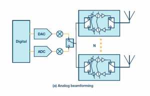
Now let’s consider the various approaches to beamforming: analog, digital, and hybrid, as shown in Figure 2. I’m sure we are all familiar with the concept of analog beamforming as this topic has been quite popular in the literature in recent years. Here we have data converters translating the digital signals to and from broadband baseband or IF signals, connecting a radio transceiver performing the upconversion and downconversion processes. At RF (for example, 28 GHz), we split the single RF path into several paths where we perform the beamforming by controlling the phase of each path so that a beam is formed in the far field in the direction of the intended user. This enables a single beam to be steered per data path, so in theory we can serve one user at a time with this architecture.
The digital beamformer is exactly what it sounds like. The phase shift is purely implemented in the digital circuitry and then fed to the antenna array through an array of transceivers. Simply speaking, each radio transceiver is connected to a single antenna element, but in practice there could be several antenna elements per radio depending on the desired sector shape. The digital approach enables the highest capacity and flexibility and enables the roadmap to multi-user MIMO at millimeter wave frequency, similar to mid band systems. It is highly complex and, given currently available technology, will consume an excessive amount of dc power both in RF and digital circuits. However, as technology evolves in the future, digital beamforming will emerge for millimeter wave radios.
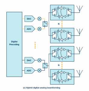
The most practical and effective beamforming approach in the near term is the hybrid digital-analog beamformer, which essentially combines digital precoding and analog beamforming to create several beams simultaneously in a space (spatial multiplexing). By directing power toward the intended users with narrow beams, the base station can reuse the same spectrum to simultaneously serve more than one user in a given timeslot. While there are a few different approaches to the hybrid beamformer reported in the literature, the subarray approach shown here is most practically implemented and is essentially a step and repeat of analog beamformers. Currently, reported systems support from 2 up to 8 digital streams in practice, which can be utilized to simultaneously support individual users, or alternatively provide 2 or more layers of MIMO to a lesser number of users.
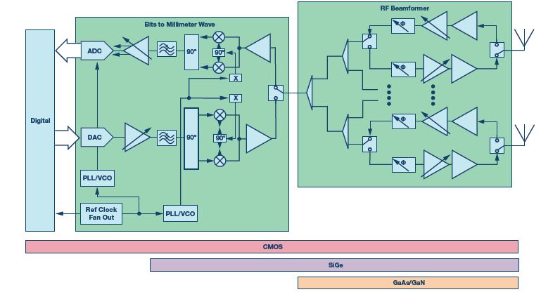
Let’s dive a little deeper into the technology choices for the analog beamformer, the building block upon which the hybrid beamformer is constructed as shown in Figure 3. For the treatment here, we have segmented the analog beamforming system into three blocks: digital, bits-to-millimeter wave, and beamformer. This is not the way a practical system will be partitioned as one would place all millimeter wave components in close proximity to mitigate losses, but the reason for this division will become obvious shortly.
 The beamformer function is driven by many factors including segment shape and reach, power levels, path loss, thermal constraints, etc., and is the section of millimeter wave systems that requires some flexibility as the industry learns and matures. Even then, there will continue to be a variety of transmit power levels required to address deployment scenarios ranging from small cell to macro. On
 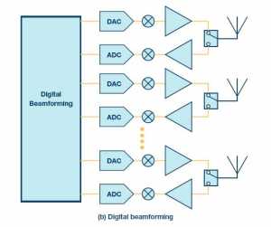 the other hand, the bits to millimeter wave radio for a base station requires much less flexibility and can largely be derived from the current Release 15 specification.3 In other words, a designer can reuse the same radio in conjunction with several beamformer configurations. This is not unlike current cellular radio systems where the small signal section is common across platforms and the front end is more tailored per use case.
We have mapped the progression of possible technologies for the signal chain as we move from digital toward the antenna. Certainly, the digital and mixed signal are produced in fine line bulk CMOS processes. Depending on the requirements of the base station, the entire signal chain may be developed in CMOS or, more likely, in a mix of technologies to provide the optimum performance for the chain. For example, a common configuration is to use CMOS data converters with a high performance SiGe B i CMOS IF-to-millimeter wave conversion. The beamformer may be implemented in several technologies as shown, depending on the system requirements, as we will discuss next. Depending on the choice of antenna size and transmit power requirements, it may be possible to implement a highly integrated silicon approach, or it may be a combination of silicon beamformer with discrete PA and LNA.
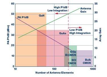
An analysis of the relationship between transmitter power and the choice of technology has been presented in previous works and will not be repeated in depth here. However, to summarize that analysis, we have included a graph in Figure 4. The selection of power amplifier technology is based on the combined consideration of required transmitter power, the gain of the antenna (number of elements), and the RF power generating capability of the selected technology. As shown in the graph, the desired EIRP may be accomplished with fewer antenna elements using II-V technologies in the front end (low integration approach) or by using a silicon-based, high integration approach. Each approach has advantages and disadvantages, and the practical implementation comes down to engineering trade-offs of size, weight, dc power consumption, and cost. To generate an EIRP of 60 dBm for the case derived in Table 1, the analysis in the presentation “Architectures and Technologies for the 5G mmWave Radio” concluded that the optimum antenna size is between 128 and 256 elements, with the lower count enabled by GaAs power amplifiers, while the larger one is achievable in all-silicon beamformer RF IC-based technology.
Now let’s examine the problem from a different perspective. 60 dBm EIRP is a commonly quoted EIRP target for FWA, but the number can be higher or lower depending on the desired reach of the base station and the surrounding environment. Given the high variation in deployment scenarios, whether the area is highly treed, or composed of street canyons, or wide open spaces, there will be a large range of path loss to contend with on a case by case basis. For example, in a dense urban deployment where LOS is assumed, the EIRP target may be as low as 50 dBm.
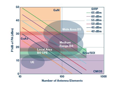
There are definition and published specifications, as well as transmit power limits, from the FCC by equipment class and here we follow the 3GPP terminology for base stations. As illustrated in Figure 5, the class of equipment more or less defines the choice of technology for the power amplifier. While not an exact science, we can see that the mobile user equipment (handset) is well suited for CMOS technology and a relatively low antenna count can achieve the required transmitter power. This type of radio will need to be very highly integrated and power efficient to meet the needs of portable equipment. The local area base station (small cell) and consumer premise equipment (transportable power) share similar requirements and span a range of technologies from CMOS on the low end of transmitter power requirements to SiGe Bi CMOS for the higher end. Medium range base stations are ideally suited for SiGe B i CMOS technology to achieve a compact form factor. At the high end, for wide area base stations, there is a range of technology that may be applied, and it comes down to the trade-offs of antenna size and technology cost. While SiGe Bi CMOS can be applied in the 60 dBm EIRP range, GaAs or GaN power amplifiers are more practical for higher power.
and choice of semiconductor technology for an antenna with 60 dBm of EIRP.
The snapshot in Figure 5 is of current technology, but much progress is being made in the industry and technology continues to improve. As mentioned in the “Architectures and Technologies for the 5G mmWave Radio” presentation, one of the key challenges for the designer is to improve the dc power efficiency for millimeter wave power amplifiers.
As new technologies and PA architectures emerge, the curves above will shift, and more highly integrated structures will be available for the high power base stations. A good overview of advancements in PA technology is presented in the presentation “A Short Survey on Recent Highly Efficient cmWave 5G Linear Power Amplifier Design.
To summarize the beamformer section, let’s reiterate the point made above. Currently there is not a one-size-fits all approach and one may need to design a variety of front-end designs to address the various use cases from small cells to macros.
Millimeter Wave Radio: From Bits to Millimeter Wave and Back
transmitter power.
Let’s move on now to the bits-to-millimeter wave radio in more detail and explore the challenges in this section of the system. It’s critical to translate the bits to millimeter wave and back with high fidelity to support high order modulation techniques such as 64 QAM and possibly as high as 256 QAM in future systems. One of the main challenges for these new radios is bandwidth. The 5G millimeter wave radios must nominally process 1 GHz of bandwidth or possibly higher depending on how the spectrum is allocated in practice. While 1 GHz of bandwidth at 28 GHz is a low relative (3.5%) bandwidth, that same bandwidth at an IF of, say, 3 GHz is much more challenging to design for and requires some leadingedge technology to achieve a high performance design.
Figure 6 illustrates an example of a block diagram for a high performance bits-to-millimeter wave radio based on components form the Analog Devices’ broad RF and mixed-signal product portfolio. This signal chain has been demonstrated to support contiguous 8× 100 MHz NR carriers at 28 GHz with exceptional error vector magnitude (EVM) performance. More details on this signal chain and its’ demonstrated performance can be found in the Analog Devices video, 5G Millimeter Wave Base Station.
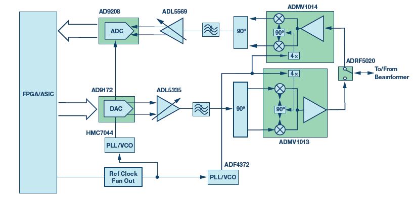
Let’s consider data converters. In the example in Figure 6, we show direct high IF transmitter launch and high IF receiver sampling used, where the data converters are launching and receiving at the intermediate frequency. The IF needs to be as high as can be reasonably achieved to avoid unwieldly image filtering at RF, driving the IF frequency to 3 GHz and above. Fortunately, leading edge data converters are capable of operating at this frequency. The AD9172 is a high performance, dual, 16-bit DAC that supports sample rates up to 12.6 GSPS. The device features an 8-lane, 15 Gbps JESD204B data input port, a high performance, on-chip DAC clock multiplier, and digital signal processing capabilities supporting broadband and multiband direct to RF signal generation up to 6 GHz. In the receiver we show the AD9208, a dual, 14-bit, 3 GSPS ADC. The device has an on-chip buffer and a sample-and-hold circuit designed for low power, small size, and ease of use. This product is designed to support communications applications capable of direct sampling wide bandwidth analog signals of up to 5 GHz.
In both the transmit and receive IF stages we suggest digital gain amp- lifiers that convert from single to balanced and vice versa to avoid the use of baluns. Here we show the ADL5335 in the transmit chain and the ADL5569 in the receive chain as examples of high performance broadband amplifiers.
For the upconversion and downconversion between IF and millimeter wave, we have recently introduced both a silicon-based broadband upconverter, the ADMV1013, and a downconverter, the ADMV1014. These broadband frequency conversion devices operate from 24.5 GHz to 43.5 GHz. This broad frequency coverage allows the designer to address all of the currently defined 5G millimeter wave spectrum bands (3GPP bands n257, n258, n260, and n261) with a single radio design. Both support an IF interface up to 6 GHz and two frequency conversion modes. As shown in Figure 6, both devices include an on-chip 4× local oscillator (LO) multiplier with LO input ranging from 5.4 GHz to 11.75 GHz. The ADMV1013 supports both direct conversion from baseband I/Q to RF and single sideband upconversion from IF. It provides 14 dB of conversion gain at a high output IP3 of 24 dBm. If implemented in a single sideband conversion, as illustrated in Figure 6, the device provides 25 dB of sideband suppression. The ADMV1014 supports both direct conversion from RF to baseband I/Q and image reject downconversion to IF. It provides a conversion gain of 20 dB with a noise figure of 3.5 dB and an input IP3 of –4 dBm. The sideband suppression in image reject mode is 28 dB.
The final component in the RF chain is the ADRF5020 broadband silicon SPDT switch. The ADRF5020 provides both a low insertion loss of 2 dB and high isolation of 60 dB at 30 GHz.
Finally, let’s discuss the frequency sources. Given that the local oscillator may be a large contributor to the EVM budget, it’s important to use a source with very low phase noise for the millimeter wave LO generation.
The ADF4372 is a wideband microwave synthesizer with an industryleading integrated PLL and ultralow phase noise VCO with output capable of 62.5 MHz to 16 GHz. It allows for the implementation of fractional-N or integer-N phase-locked loop (PLL) frequency synthesizers when used with an external loop filter and an external reference frequency. VCO phase noise at 8 GHz is an impressive –111 dBc/Hz for 100 kHz offset and –134 dBc/Hz at 1 MHz offset.
Summary
The block diagram in Figure 6 is a good starting point for any designer considering a millimeter wave design in the 28 GHz and 39 GHz bands and suitable for use with a variety of beamforming front ends requiring a high performance broadband radio. There are also many components listed in ADI’s RF, Microwave, and Millimeter Wave Products Selection Guide that may be of interest to the designer for other signal chain architectures or for similar high frequency applications.
Millimeter wave radios have seen great progress in recent years, moving out of the lab to field trials with commercial deployments that are launching in the coming months. The evolving ecosystem and emerging use cases require some flexibility in the beamforming front end, but as discussed there are suitable technologies and approaches to choose from for the near antenna designs. The broadband nature of the radio (bits to millimeter wave) demands leading-edge technology, but silicon-based technology is quickly evolving to meet the requirements in the mixed-signal and small signal domains. A high performance radio design example has been presented based on currently available components.
As the 5G ecosystem continues to evolve, Analog Devices will continue to bring to bear our leading-edge technologies and signal chain solutions to enable our customers to develop differentiated systems for the emerging 5G millimeter wave market.