


Description
The automotive camera reference design offers a complete solution for a 76-GHz to 81-GHz radar sensor module. The onboard power supplies convert the automotive battery input to the required rails for the radar analog front end (AFE), processors, and controller area networking with flexible data rate (CANFD) transceiver. After processing, the object data transmits over the included CAN-FD physical layer (PHY).


Features
- Space-Optimized Design Fits on Single PCB
- (Approximately 50 mm × 71 mm)
- Power Supply Optimized for Small Size and High
- Efficiency
- Single-Chip 76- to 81-GHz Automotive Radar Sensor Integrates DSP and MCU and Provides
- Object Data Over CAN-FD
- Wide VIN 36-V OFF Battery Supply Tolerates up to 42 V
- Diagnostic and Monitoring Functions for ASIL B Applications
Applications
- ADAS Radar Systems
- Blind Spot Detection (BSD)
- Lane Change Assist (LCA)
- Front/Rear Cross-Traffic Alert (F/RCTA)
- Autonomous Emergency Braking (AEB)
- Adaptive Cruise Control (ACC)
1 System Description
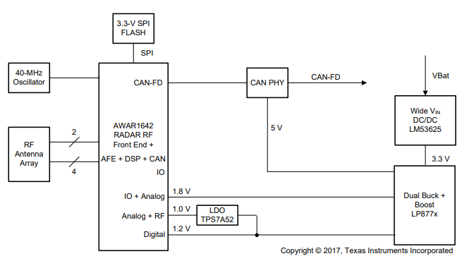
Radar sensors are a requirement for many automotive safety systems. Locating these sensors in bumpers and side mirrors can be difficult. A very small sensor simplifies the process of meeting these market demands and provides a less expensive approach to meet such requirements. This reference design addresses these concerns by combining a single-chip, 76- to 81-GHz automotive radar sensor with a CAN-FD PHY and providing the necessary power supply. All of this functionality is contained on a 50×71mm circuit board. The only two connections that the system requires are the battery power in and CAN-FD out
The battery power connects to the 12-V input terminal, J1. The wide VIN buck, LM536253-Q1, is utilized to convert this 12-V input to a 3.3-V output. The LP87702-Q1 then takes the 3.3-V input and creates 5.0- V, 1.8-V, and 1.24-V rails. To ensure a low-noise supply, the TPS7A52-Q1 low-dropout linear regulator (LDO) creates a clean 1-V rail for the radio frequency (RF) section of the radar.
The radar section of this design utilizes a printed-circuit-board (PCB) etched antenna with two transmit elements and four receive elements. By using this antenna, a modulated chirp is transmitted and reflections are sampled into the onboard digital signal processor (DSP). With this information, the sensor can record distance, angle, and velocity measurements from objects within the antenna field of view.
The design offers a feature to write out the object data to a central electronic control unit (ECU) on the CAN-FD bus at a rate of 5 Mb/s.
1.1 Key System Specifications
Table 1. Key System Specifications
| PARAMETER | COMMENTS | MIN | TYP | MAX | UNIT | |
| VIN | Supply voltage | Battery input | 4 | 12 | 42 | V |
| PTOTAL | Total power consumption | VIN = 12 V | — | 2.6 | — | W |
| CAN-FD | Data rate | — | — | — | 5 | Mb/s |
2 System Overview
2.1 Block Diagram
2.2 Highlighted Products
This reference design uses the following TI products:
- AWR1642-Q1: This integrated, single-chip frequency-modulated continuous wave (FMCW) radar sensor is capable of operation in the 76- to 81-GHz band. The device is built with TI’s low-power 45-nm RFCMOS process and enables unprecedented levels of integration in an extremely-small form factor (SFF). The AWR1642 is an ideal solution for low-power, self-monitored, ultra-accurate radar systems in the automotive space.
- LP87702-Q1: This automotive-qualified power device is optimized for radar applications with a dual high-current buck converter and 5-V boost. The high switching frequency of up to 4 MHz allows the use of small inductors and improves system performance because the second harmonic is out of the IF band of the AWR1642 sensor. The LP87702-Q1 includes diagnostics functions such as monitoring of the internal and two external rails, two programmable power-good outputs, and a window watchdog.
- TPS7A52-Q1: The TPS7A52-Q1 is an automotive-qualified, low-noise 2-A linear regulator with ultralow dropout. This linear regulator filters any power supply noise that emanates from the upstream switching supplies while minimizing dissipation through ultra-low dropout operation.
- LM536253-Q1: The LM536253-Q1 synchronous buck regulator is optimized for automotive applications and provides an output voltage of 5 V, 3.3 V, or an adjustable output. Advanced high-speed circuitry allows the LM53625-Q1/LM53635-Q1 to regulate from an input of 18 V to an output of 3.3 V at a fixed frequency of 2.1 MHz. Innovative architecture allows this device to regulate a 3.3-V output from an input voltage of only 3.55 V. All aspects of the LM53625-Q1/LM53635-Q1 are optimized for automotive and performance-driven industrial customers. An input voltage range up to 36 V, with transient tolerance up to 42 V, eases input surge protection design.
- TCAN1042GV-Q1: This automotive CAN transceiver meets the ISO11898-2 (2016) high speed CAN physical layer standard.
The following subsections provide more information on each device and why they have been chosen for this application.
2.2.1 AWR1642-Q1 CMOS RADAR
AWR1642 is a single-chip radar sensor built with four receivers and two transmitters. Built with RFCMOS technology, the device integrates the RF and analog subsystem with the digital subsystem to deliver low power in an SFF for ultra-short-range radar (USRR) and short-range radar (SRR) applications. The device is based on closed-loop phase-locked-loop (PLL) architecture for precise and linear chirp synthesis. The device includes a built-in radio processor (BIST) for RF calibration and safety monitoring. Based on complex baseband architecture, the sensor device supports an intermediate frequency (IF) bandwidth of 5 MHz with reconfigurable output sampling rates. Integration of an ARM Cortex-R4F processor and Texas Instruments C674x DSP (fixed and floating point), along with 1.5MB of on-chip RAM, enables highlevel algorithm development.
2.2.2 LP87702-Q1
The LP87702x-Q1 contains two high-current (up to 3.5 A) buck converters and a 5-V boost for CAN supply. The device supports remote voltage sensing to compensate IR drop between the regulator output and the point-of-load (POL), which improves the accuracy of the output voltage. The device is either controlled by an I2C-compatible serial interface, enable signal, or both.
The 4-MHz high-switching frequency of the LP87702D-Q1 allows the use of small inductors and improves system performance by pushing the second harmonic out of the maximum IF band of the AWR1642 device. To further protect the system from electromagnetic interference (EMI), the buck and boost converters are programmed to forced pulse-width modulation (PWM) mode for a fixed switching noise spectrum. When an external clock is provided, the device automatically synchronizes buck and boost clocks to the external clock.
The integrated diagnostic functions of the LP87702D-Q1 help to reduce the radar solution size. The validity of the internal regulator output voltages, 3.3-V input, and two external rails can be monitored through two programmable power-good outputs. The device also includes a window watchdog with programmable open and close times and reset output.
2.2.3 TPS7A52-Q1
The combination of low-noise (4.4 μVRMS), high power-supply rejection ratio (PSRR), and high output current capability makes the TPS7A52-Q1 ideal to power noise-sensitive components, such as the RF portion of an automotive radar sensor.
The RF supply rails (1.3 V) can be overridden and supplied with an external 1.0-V voltage regulator; however, this supply must be free of excessive noise, which can be detrimental to system performance. The TPS7A52-Q1 has high PSRR over an extended bandwidth to ensure that any upstream switching noise at or above 1 MHz is attenuated effectively. The TPS7A52-Q1 also has very low levels of intrinsic noise (as low as 4.4 μVRMS) through the use of a noise-reduction capacitor. Together, these qualities make this device a good choice to ensure a quiet power supply.
Additionally, this device is capable of low dropout operation with the use of a higher bias rail. Use of this rail limits the minimal power dissipated across the LDO that typically heats up the board and surrounding components. Rather than dissipate power with the internal LDO from 1.3 V to 1.0 V, using the TPS7A52Q1 enables a 1.2-V to 1.0-V conversion and cuts the dissipation by 33 %.
2.2.4 LM536253-Q1
The LM536253-Q1 is designed to support a smaller solution size and run at cooler temperatures in a application, which is a combination of package technology and higher overall efficiency in operation. Using several techniques to minimize switch noise and minimized parasitic impedance, this device offers low noise emission which helps to lower system electromagnetic compatibility (EMC) and assist with the ease of design. The DC/DC converter is optimized for out-of-standard regulation conditions, which can either be fault conditions or normal operation (like cold crank and load dump). The LM536253-Q1 offers the full capability to assist front-end automotive power supply designs.
2.2.5 TCAN1042GV-Q1
This automotive CAN transceiver meets the ISO11898-2 (2016) high-speed CAN physical layer standard. This PHY has a low power standby mode with remote wake request and many protection features to enhance device and network robustness. This PHY was chosen for its simplicity and small size.
2.3 Design Considerations
2.3.1 PCB and Form Factor
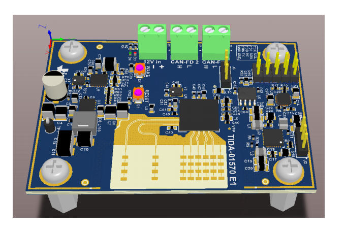
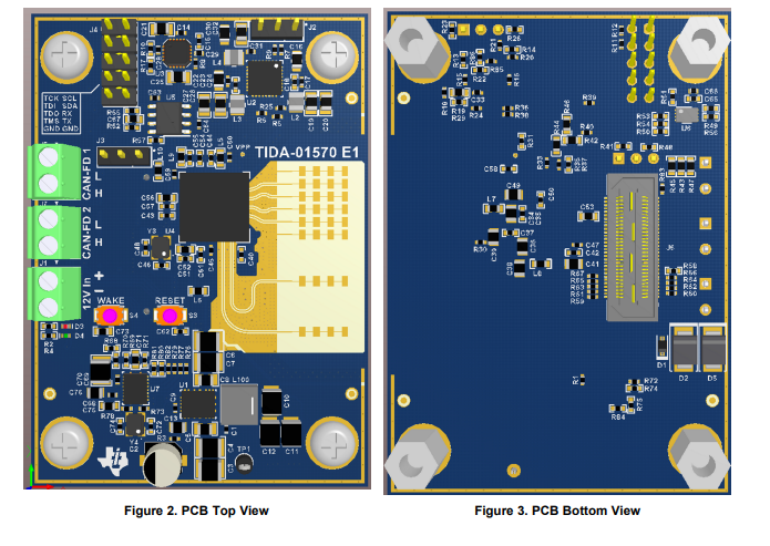
This reference design is not intended to fit any particular form-factor. The only goal of the design with regards to the PCB is to make a compact solution that serves as a fully-featured automotive radar sensor. With the mounting holes, the board measures roughly 50 mm × 71 mm (2 in × 2.8 in). Figure 2 and Figure 3 show the top view and bottom view of the PCB.
 2.3.2 Power Supply Topology
As the previous Figure 1 shows, the radar sensor reference design is intended to connect directly to the vehicle battery. The voltages required for the design are:
- 5 V for CAN-FD PHY
- 3 V for radar I/O
- 8 V for radar analog, RF, VCO, and CMOS
- 2 V for radar digital and SRAM
- 1 V or 1.3 V for radar analog and RF
An automotive battery supplies the power input to this sensor; therefore, the design requires a wide VIN buck that can tolerate up to 40 V as the first stage of the power supply. Use a multi-rail power supply, which has been specifically designed for this application, to create the 5-V, 1.8-V, and 1.2-V rails. The designer has the option to provide the radar analog and RF supply as a 1.3-V input to the LDO inside the AWR1642 device. Another option is to directly supply the radar analog and RF supply as a low noise 1- V rail. The latter option reduces the power dissipated by the AWR1642 device. This option may also reduce the total system power, depending on the system architecture. For this design, supply the radar analog and RF supply externally with a low-noise LDO. By raising the 1.2-V rail to 1.24 V, enough headroom becomes available to cover the dropout on the LDO that produces the 1-V output. This action also reduces the power dissipated in the LDO by using 1.24 V as the input to the LDO, rather than the next higher voltage rail, 1.8 V.
2.3.2.1 AWR1642 Power Supply Considerations
The AWR1642 device utilizes four power rails for its operation: a 1.2-V digital supply, 3.3-V IO supply, 1.8V analog supply, and 1-V RF supply. The average current consumption depends on the chirp profile and frame configuration used; for example. a 1Tx , 4 Rx use case with a 50% duty cycle and DSP processing consumes approximately 1.9 W of average power.
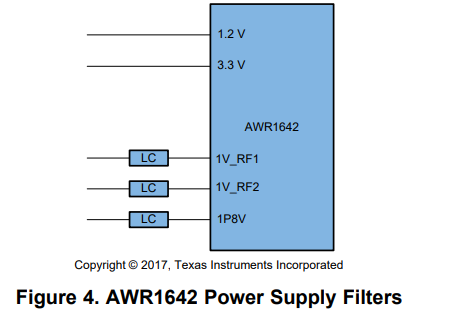
In a case where the 1-V supply is derived from the 1.2 V using a regulator (such as in this reference design), the 1.2 V (1.24 V) of available current must include both 1.2-V and 1-V rail currents. Figure 4 shows a block diagram of the AWR1642 power supply filters.
One of the key concerns when using the switching regulators for the power supply is to prevent the switching frequency of the regulator from coupling onto the analog circuitry through the supply or ground. At a 4-MHz switching frequency, the AWR1642 can tolerate approximately 35.5-uVRMS ripple on the 1.8- V supply to keep the spur in the RX spectrum of less than –120 dBm (at the LNA input). The following steps offer ways to reduce the supply ripple level:
- Use LC filtering on the analog and RF supplies (1.8 V and 1 V).
- Some of the output voltage ripple of a switching buck regulator is caused by the inductor ripple current charging and discharging the output capacitor. Minimize this inductor ripple current by using a high switching frequency, in this case 4 MHz. The recommended inductance for LP87702-Q1 buck regulators is 0.47 µH.
- A higher output capacitance reduces the output voltage ripple and also improves load step behavior. Use ceramic capacitors with low to minimize ripple. The RESR is frequency dependent (as well as temperature dependent); make sure the value used for the selection process is at the switching frequency. Use the point-of-load capacitors to further decrease the ripple voltage and improve load transient performance.
- Use the LC filter to continue filtering the output from the regulator. Place a series ferrite bead on the supply path, along with the decoupling capacitors of the supply, so that they can act as an LC filter to reduce the ripple amplitude. Choose the values such that the corner frequency of the LC filter is much lower than the switching frequency. For example, in this design, the LP87702 switches at a 4- MHz frequency. The LC filter is designed with the part number BLM18KG121TH1 to provide a cutoff frequency of approximately 120 KHz with the decoupling capacitors on the 1.8-V supply rail.
, processors, and controller area)
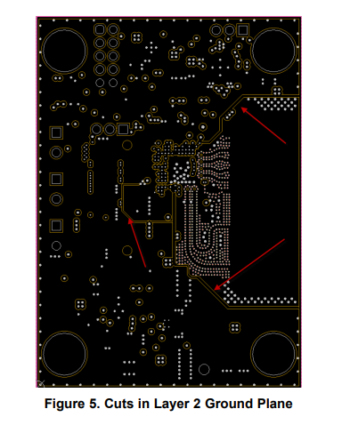
- By providing ground cuts, the designer can reduce the interference of the switching currents for the regulator and the analog currents on the AWR1642 device (see Figure 5). The circuits most vulnerable to ripple are the XTAL lines, VOUT_14SYNTH , VOUT_14APLL, VIN_18VCLK, and VIN_18VCO supplies.
2.3.2.1.1 Wide VIN Buck
Under start-stop or cold-crank conditions, the voltage can drop quite dramatically—and to a level that causes the buck converter to go out of regulation. Some instances may require the designer to use a boost converter in the circuit to assist the system. If designing the power supply to support sudden voltage drops, the designer may be able to account for the cost of the boost, as well as the cost, space, and power consumption associated with the additional components.
A combination of a nearly 100% duty cycle, very-short minimum OFF-time, and a low RDS(ON) high-side field-effect transistor (FET) resistance enables the power supply to support a deep dropout of less than 0.6 V under a full load and full operating temperature range, all while maintaining regulation for downstream power supplies without adding additional design complexity. This feat is made possible by using the LM53625-Q1 under typical and extreme conditions in an automotive system.
Maintaining regulation and stopping the power supply from becoming unstable is critical in automotive power supplies around the minimum drop-out and high VIN conditions. System-related conditions like cold crank or even load dump from faulty alternators can affect the regulation and output power. Support for low dropout requires that the device output does not oscillate. This oscillation would translate into highfrequency noise and can cause disturbances elsewhere in the system. The LM53625-Q1 is used here because it is designed to support very-low TMIN-ON and TMIN-OFF conditions. Stable control of the power supply is critical and smooth operation into and out of a desired regulation range is required, as this controls the noise that is generated.
2.3.2.1.2 Reducing EMI
The selection of available, low EMI power supplies is increasingly important due to many factors, including the progressively complex wire harnesses used in automobiles and the number of ECU nodes to add to the system. Each harness wire and each ECU has the ability to create noise that can be transmitted around the automobile and affect other applications. Given the increasing number of safety applications, the ability to offer low EMI is highly desirable. Several techniques can be used in the design of the power supply to minimize EMI.
One technique to lower the EMI is to choose a converter in a package that is optimized for layout placement and positioning of the passive components used in regulation and filtering. LM53625-Q1 uses a pinout that offers symmetrical placement of the high-frequency input capacitors, which are grounded on either side of the switch node. This placement creates reduced inductance between ground (GND) and the switch, which cancels any noise. Additionally, by constructing the package in a certain manner, the designer can remove the parasitic loop inductance and capacitance inside the package and reduce the switch-node ringing, which is a major contributor to noise generation. The general idea is to reduce the noise at the source to avoid any problems caused by additional components. The LM53625-Q1 uses a flip chip package construction that
removes the bond wires, which can, in some instances, add to the noise and degrade dropout and efficiency.
Another technique for reducing noise in the system is spread-spectrum technology, which modulates the central switching frequency and suppresses the harmonics and sub-harmonics. Spread-spectrum is very effective for reducing the overall noise peaks, but does not influence the noise floor due to the spreading of the noise, as the name suggests. However, because spread-spectrum helps with high-frequency harmonics, it can help meet the stringent original equipment manufacturer (OEM) standards for EMI, simplify printed-circuit board (PCB) designs, and reduce filtering component size and cost. The LM53625-
Q1 offers a version with and without spread spectrum to provide flexible options to the customer across multiple designs and systems.
2.3.2.1.3 Antenna
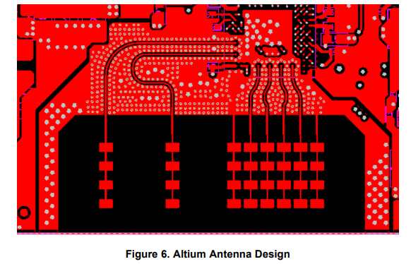
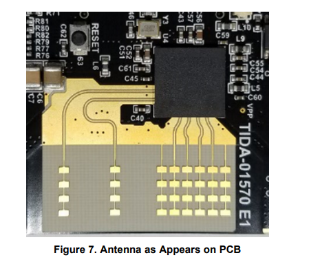
This reference design includes onboard-etched antennas for the four receivers and two transmitters that enable tracking multiple objects with their distance and angle information. This antenna design utilizes the estimation of distance and elevation angle, which, in turn, enables object detection in a two-dimensional plane. Figure 6 and Figure 7 show the PCB antennas.
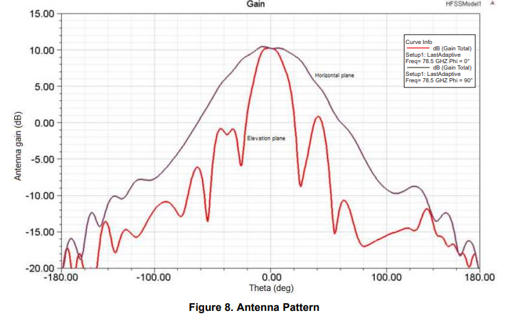
The antenna peak gain is greater than 9 dBi across the operating frequency band of 76 GHz to 81 GHz. The peak output power with the antenna gain is less than 55 dBm equivalent isotropically radiated power (EIRP), as required by the European regulations. Figure 8 shows the radiation pattern of the antenna in the horizontal plane (H-plane Phi = 0°) and elevation plane (E-plane Phi = 90°).
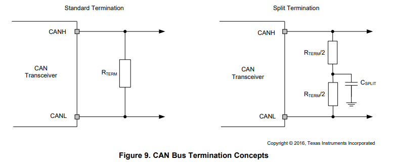
2.3.2.1.4 CAN Termination
The ISO 11898 standard specifies the interconnect as a twisted pair cable (shielded or unshielded) with 120-Ω characteristic impedance (ZO). Resistors equal to the characteristic impedance of the line must be used to terminate both ends of the cable to prevent signal reflections. Unterminated drop lines (stubs) connecting nodes to the bus must be kept as short as possible to minimize signal reflections. The termination may be on the cable or in a node, but if nodes may be removed from the bus, the termination must be carefully placed so that two terminations always exist on the network. Termination may be a
single 120-Ω resistor at the end of the bus, either on the cable or in a terminating node. If the designer wishes to filter and stabilize the common-mode voltage of the bus, then split termination may be used (see Figure 9). Split termination improves the electromagnetic emissions behavior of the network.
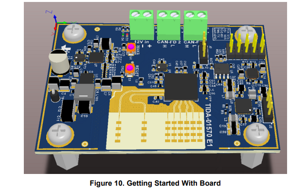
3 Getting Started Hardware
Connect the TIDA-01570 reference design to a 12-V nominal “battery” supply using the screw terminals on J1 (see Figure 10). The object data output is available on the CAN-FD signals on J5.
3.1 AWR1642 Initialization: Board Programming
Now that the board is powered with the 12-V connection, a program must be loaded into the FLASH. This program executes each time the board boots and the AWR16 is released from RESET. TI provides a mmWave Software Development Kit (SDK). This SDK is a unified software platform for the AWR1x family of mmWave sensors, which enable evaluation and development. The use of this design environment is covered in the documentation for the mmWave SDK: MMWAVE-DEVPACK and MMWave Demo Visualizer User’s Guide. The following procedure is for loading a binary file.
• Use UniFlash with an FTDI cable to load the program.
• During the following procedure, the AWR1642 universal asynchronous receiver/transmitter (UART) RX/TX pins are connected to the PC through a USB cable using an FTDI cable. The specific cable used is the UART to USB: TTL-232R-RPI CABLE USB-SERIAL RASPBERRYPI. Be sure to install the correct PC drivers for the selected USB and UART cables.
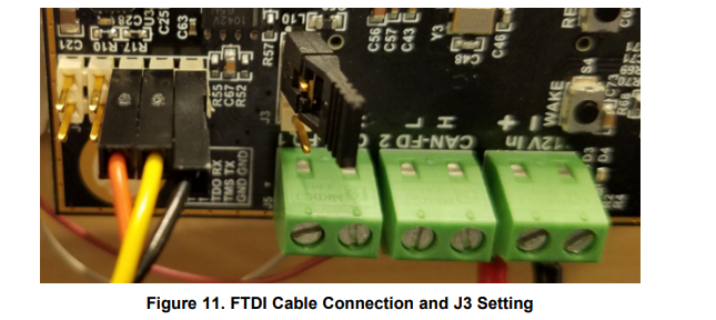
3.2 Sense-on-Power (SOP) Jumpers
As the previous Figure 11 shows, the J3 jumper is used to configure the device into FLASH programing mode. Two additional resistor dividers are used to configure the AWR1642 device at start-up. These SOP configuration options are shown at the bottom of sheet 2 of the schematic (available for download in Schematics). These lines are sensed only during boot up of the AWR device. Table 3 provides a description of the SOP modes. A “0” represents pulling the pin low and a “1” represents pulling the pin high.
Article Courtesy: Texas Instruments