


At a time when IoT and the cloud are facts of life and all the rage in the trade press, advances are still being made in old fashioned electronics components by adopting the most modern technologies and optimizing designs. One example is analog-to-digital converters, which can now achieve 32-bit resolution at rates exceeding one megasample per second (MSPS), burning through traditional metrology benchmarks.
These high precision converters can display better than 16-bit resolution, specify comparable static and dynamic characteristics, and they have made their way into a number of process control applications, programmable controllers, the control of large electric motors, and the transport and distribution of electrical energy, in addition to their more exclusive domains of instrumentation and large general acquisition systems (testing, equipment qualification) or specialized systems (digital imaging for medical applications and spectroscopy).


Several ADC architectures compete at present in terms of precision and, depending on their needs, the choices align with analog-to-digital conversion principles, successive approximation register (SAR) vs. Σ-Δ, which are respectively capable of resolutions of up to 24 bits and more for a few MSPS, and 32 bits at several hundred kSPS. When faced with these levels of resolution and precision where the useful dynamics offered by these converters easily exceeds the magical barrier of 100 dBFS (full scale), users face a real challenge in the design of analog conditioning circuitry for the signals to be digitized, as well as the associated antialiasing filters. Sampling rates and filtering techniques have evolved significantly over the past two decades and it is now possible to use a combination of analog and digital filters to achieve a better compromise between performance and complexity.
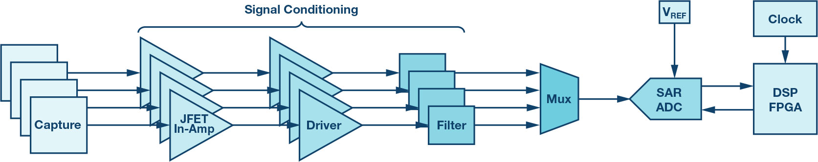
Figure 1 shows a typical example of this kind of partition for a data acquisition system. After conditioning the differential or nondifferential signals (amplification, scaling, adaptation and translation of levels, etc.), the latter is filtered before digitization to satisfy the Nyquist criterion. Depending on the oversampling rate of the ADC(s), additional digital filtering is used to comply with the specifications of the acquisition system.
Many of the aforementioned applications employ state-of-the-art high resolution ADCs due to the increased demand for very wide input dynamics. With the increased dynamics, one can expect system performance improvements along with a resulting compaction of the analog conditioning chain and a reduction in congestion and energy consumption, or even material costs.
Oversampling and Its Benefits
Before the advent of very fast, high resolution analog-to-digital coders, the dynamics problem was solved at the conditioning chain level by using fast programmable gain amplifiers, even faster comparators, and/or the paralleling of several ADCs, topped off with suitable digital processing to enable digitization of strong signals and discriminate small amplitudes near the noise level. In these antiquated and now obsolete architectures, this translated into complex circuits that were difficult to develop and were limited in terms of linearity, bandwidth, and sampling frequency.
Today’s alternative is to apply oversampling techniques by exploiting the high sampling rates offered by modern and more economical ADCs. The action of sampling a signal at an FSE rate higher than the minimum imposed by the Nyquist theorem enables performing a gain operation through processing and increasing the signal/noise ratio of an encoder, and consequently increasing the number of effective bits. Indeed, the quantization noise and thermal noise are assimilated into a white noise that spreads uniformly over the entire Nyquist band and beyond.
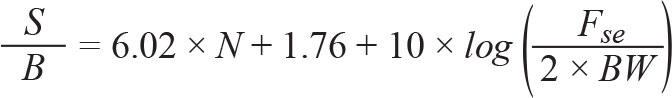
After oversampling, restricting the useful band by filtering and operating strictly at the minimum required sample rate, or 2 × BW, permits a reduction of noise energy by 3 dB for each octave of band reduction, as indicated in Figure 2. In other words, an oversampling factor of 4 ideally provides a theoretical increase in the signal-to-noise ratio of 6 dB; that is, one additional bit, as expressed by Equation 1:

In summary, oversampling has two advantages, namely an improvement in the signal-to-noise ratio, and a relaxation of the demands placed on the antialiasing analog filter before the ADC.
Antialiasing Filter: The Partition Dilemma
Ideally, the filters associated with the ADCs, and particularly those tasked with the problem of aliasing the spectrum, must have an amplitude response with the flattest possible bandwidth compared to their precision, as well as an out-of-band attenuation adequate to their dynamics. The transition band should generally be as steep as possible. Thus, these antialiasing, low-pass filters must have characteristics that enable them to eliminate parasitic images, noise, and other spurious tones. Depending on the application, significant attention should also be given to the phase response, and any excessive phase shift should be compensated. Many recommendations are considered elementary, but become very difficult to implement when they must be combined with the requirements of a specified 24- or 32-bit converter with an integral nonlinearity error of only a few LSBs and other similar static and dynamic parameters.
The interest in oversampling, as stated earlier, assumes its full importance here due to its beneficial effects not only on the signal-to-noise ratio, but also on the accompanying relaxation of the specifications for the analog antialiasing filter and its cutoff frequency. As shown in Figure 3, oversampling spreads the transition band between the cutoff frequency at –3 dB and the beginning of the stop band.

cutoff frequency a –3 dB and the beginning of the stop band.
The current technology provides for highly precise SAR ADC conversion rates that have increased considerably in recent years, and currently reach from over 1 MSPS up to 15 MSPS for 18-bit resolution. By comparison, wideband Σ-Δ ADCs with equivalent resolution are slower by almost an order of magnitude and suffer from significant latency, as well as ripple in the pass band that is too high for consideration in some applications such as data acquisition systems or other measuring instruments. These latter are fundamentally characterized by their overall metrological precision, which relates both to the static (dc) and dynamic (ac) parameters, and therefore the converters and the accompanying analog conditioning circuitry in these systems must have top tier specifications.
These include the usual characteristics, such as offset, gain and corresponding drift errors, integral nonlinearity (INL), and differential (DNL) errors, but also include signal-to-noise ratio (SNR), harmonic distortion, and spurious tones (spurious-free dynamic range, SFDR). The SAR ADCs have a clear competitive advantage (INL) in some of these parameters, as well as the transient response and analog input overload, and their zero delay latency, which guarantees the operation of multiplexed input systems or triggering of acquisition in one shot mode.
Conversely, most SAR ADCs do not include a digital filter except for the LTC2512 and LTC2500-32, and their operation is therefore not impeded or limited by some unavoidable digital low-pass filtering that results in a compromise between computational accuracy, band-pass ripple, attenuated band rejection, propagation time, and power consumption. In most cases, the user has no control over the values of the coefficients of the internal filters for these Σ-Δ converters and must make do.
The LTC2378-20: First 20-Bit SAR ADC on the Market
In the race for performance, during 2014, Linear Technology (now part of Analog Devices) caught its competitors up short by offering its customers the first successive approximation ADC with 20-bit resolution and nothing less than linearity. The LTC2378-20 is an exceptional converter that still holds its own against the best of all other competitors that are closing in on MSPS.
The AD4020, the one-time frenemy of the LTC2378, is Analog Devices’ first 20-bit SAR ADC capable of digitizing 10 V p-p differential signals at 1.8 MSPS. It combines low noise and low energy consumption with all the features of the LTC2378: dynamic compression, clamping circuitry, charge transfer compensation allowing the use of low power precision amplifiers (high-Z mode), etc. Powered at 1.8 V, it consumes only 15 mW at 1.8 MSPS. Its record conversion time of 350 ns allows for some leeway to extend the acquisition time or for reading data. It is enclosed in a 10-lead MSOP or 10-lead QFN casing that it shares with the other 16- to 18-bit members of the AD40xx family. Its specifications and operation are guaranteed over the temperature range from –40°C to +125°C.
With sampling rates of 1 MSPS and 1.8 MSPS, respectively, the LTC2378-20 and AD4020 offer significant possibilities for oversampling, particularly with respect to the audio band or beyond. To do this, a customized decimation filter must be implemented in an external FPGA or DSP. As mentioned earlier, the latter can be bypassed to reduce the latency to its minimum if necessary. With these primary sampling rate values and in considering the 0 kHz to 25 kHz band, the respective oversampling factors are approximately 16 or 32, and processing gains of 12 dB to 18 dB result along with a simplification of the antialiasing, low-pass filter with regard to conventional operation strictly according to Nyquist theorem.
ADC to DSP Link: Everything Is Serial
In recent years, the semiconductor industry and its coterie of designers have an obvious penchant for a reduction in component sizes, leading to a real deflation of the casing pins and conditioning almost all the digital inputs or outputs in serial form, which are required to be interfaced with SPI buses, synchronous serial ports, etc.
The converters in question here are not left with their serial interfaces used both to extract the samples and control the various functional options of the ADC. These serial interfaces are qualified to be compatible with SPI or with the DSP serial ports, but are not really so. At best, they hide the shift registers that set the rhythm of a clock signal for extracting data from the device, or to inject it during configuration.
Like all of these SAR ADCs, the LTC2378-20 and AD4020 have frequency requirements for the serial clock (SCK) to recover each 20 bits of data at the nominal sampling rate. As the phase of data reading is strictly limited to the duration of the acquisition time, which is of the order of some 300 ns, the digital activities on external access must be reduced to total silence during the conversion period, and a clock frequency of more than 60 MHz is necessary to recover all the bits from a sampling over the allotted time while respecting the sampling rate of 1 MSPS. This is a severe constraint imposed on the interface of the controller in charge of collecting the data from the ADCs, both for generating such clock frequencies, but also with respect to the time specifications to be achieved the receiver side.
The minimum SCK signal frequency of 64 MHz required by the LTC2378-20 means that it cannot be interfaced with just any general-purpose microcontroller or most DSPs with synchronous serial ports (SPORTs) that exceed the maximum frequency of barely 50 MHz, except for some members of the Blackfin family, such as the ADSP-BF533 or ADSP-BF561 that can reach 90 Mbps. Therefore, there is concern that the use of a large CPLD or FPGA associated with low jitter clock generation circuitry is essential.
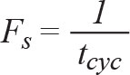
Most of the digital interfaces for the serial output SAR ADCs share more or less the same timing and logic signal patterns as shown in Figure 4. As for the SDI configuration input, apart from the cascade modes, it is sought at much lower frequencies. The equivalent full cycle time for the ADC sampling period is:
![]()
thus defining the maximum sampling frequency, consists of:
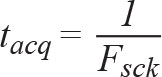
itself conditioned by the reading rate of the output data with

Fortunately, the AD4020, with its very short conversion time of 325 ns and a sampling rate of 1 MSPS, allows an acquisition time of 675 ns and consequently a serial data read frequency of less than 33 MHz, a frequency that matches that of the DSP synchronous serial ports, such as the SHARC ADSP-21479, and very low energy consumption.
An Ultra Low Power Multichannel Acquisition System
For reasons of energy consumption, precision, and flexibility in choice of operating modes, but also for commercial reasons, FPGA-based solutions cannot be considered in these lines. Only DSP floating-point processors are retained for the processing of the serial outputs from these 20-bit ADC and for realizing optimized decimation filters.
Today, there are many data acquisition systems capable of simultaneous sampling over a large number of channels. This translates into many ADCs operating in parallel, while being governed by the same controller that also has the task of collecting the data and storing it in memory for subsequent analysis.
A system constructed around SAR ADCs associated with the capabilities of a SHARC ADSP-21479, or one of its fast ADSP-21469 or ADSP-21489 versions clocked at 450 MHz, is not only conceivable but presents itself as the most pertinent in terms of performance, development time, energy consumption, and compactness. These processors have all the functions and peripherals needed to support 8 analog-to-digital digitization channels, from synchronous serial interfaces to the generation of different clock signals and triggering conversion.
Among all SHARC processors, the ADSP-21479 is the only 32-/40-bit floating-point DSP to be manufactured with a low leakage, 65 nm CMOS process, which has the advantage of substantially reducing leakage or static currents, and the evolution of which with the junction temperature is almost exponential. The dynamic current, which is a function of the frequency and activity of the processor and its peripherals, is also lower than that for standard or fast CMOS manufacturing process. The flip side is a maximum CPU frequency reduced by about 30% to 40% compared to conventional versions, nevertheless largely sufficient for the needs of such an application.
The ADSP-21479 has many peripherals including a special block called a serial input port, or SIP, that is capable of simultaneously receiving streams from eight external serial port transmitters in synchronous operation with clock and synchronization signals. In fact, it is possible to directly connect eight ADCs similar to the AD4020 directly to this interface, and thus to the processor. As shown in Figure 5, the 8 channels have their own IDP_SCK clock, IDP_FS synchronization, and IDP_DAT input signals, and their data, once deserialized, are automatically multiplexed into a 32-bit, 8-word FIFO memory before being transferred to the SHARC internal RAM, through either a 64-bit DMA packet or a read performed by the CPU.
In a DMA transfer operation, the SIP is served by a double-indexed DMA channel operating in automatic ping-pong mode. In addition, the ADSP21479 features four precision clock generators (for their low jitter) or PCGs capable of generating independent pairs of clock and synchronization signals from an internal or external source (TCXO). The frequency, period, pulse width, and phase of these stimuli are obtained by programming 20-bit internal dividers. Each PCGx generation unit provides a pair of CLK/ FS signals shared by a pair of AD4020 converters, but the clock must be silent during the conversion phase, which accounts for the presence of a logic gate that combines the IDP_FS and IDP_SCK signals to create the SCK clock. The time diagram in Figure 5 shows that once the conversion time tconv has elapsed, the 20 bits from the current sample must be read as quickly as possible, that is, at the rate of 33.3 MHz to maintain the 1 MSPS magical barrier in the sampling frequency.
About 600 ns later, the data is transferred to one of the SIP buffers and a new conversion cycle can be started using the IDP_FS or CNV signal to trigger a new conversion of the AD4020. Having a maximum 325 ns conversion time for the latter will correspond to the pulse width of the CNV signal, that is, 12 IDP_SCK clock periods or 360 ns. In summary, as shown in the timing diagram of Figure 5, 32 IDP_SCK signal periods, or a total of 960 ns, are required for a complete scan cycle, resulting in a maximum sampling rate of 1.040 MSPS.
Similarly, the ADC LTC2378-20 can be associated with an ADSP-21489 since it is capable of operating at the clocks of higher peripheral clock frequencies up to 50 MHz, and the sampling rate in this case will be 900 kSPS, as shown in Table 1. Unfortunately, the static supply current (Iddint), or leakage of the latter, is much higher than the dynamic current, which makes an unacceptably high overall consumption for this configuration by exceeding the available wattage.
Decimation Filtering
Assuming that these converters are used in oversampling mode, it is therefore necessary to provide a decimation filter tailored for the band of interest with the aforementioned performance requirements, minimizing the impact on the DSP in terms of required computing power and energy consumption. Currently, the procedure for changing the sampling rate has become a standard digital signal processing operation, and these are performed using interpolators and digital decimators. For reasons of linearity in the phase response, the low-pass decimation filter uses a finite impulse response (FIR) topology, and different topologies can be used according to the degree of efficiency sought:
- Direct or optimized FIR filters for decimation
- Cascaded multirate FIR filters (1/2 band)
- Polyphase FIR filters
Polyphase filters, whether of the FIR or IIR type, are one of the most efficient implementations of decimation or interpolation filters. Nevertheless, digital processing orthodoxy requires filtering before decimation. On this assumption, a 1/M decimation filter consists of a low-pass filter followed by a sampling frequency reduction stage (Figure 6a). The signal is filtered beforehand to avoid the aliasing of spectrum, then the samples are periodically eliminated at the rate of M–1. However, the direct implementation of these decimation filters of the conventional FIR or other structures is wasteful of resources knowing that the rejected samples result from a few tens or even hundreds of multiplication-accumulations (MACs). The use of polyphase filters decomposed into several banks of filters, or filters optimized for decimation, leads to the production of efficient filters based on certain identities such as that illustrated in Figure 6b.
With their SIMD architecture and hardware accelerator dedicated to FIR filtering, and an instruction set optimized for digital signal processing, the SHARC ADSP-21479 is particularly well positioned for the implementing these types of filters. Each SHARC processing element has a 32-/40-bit multiplier-accumulator capable of providing 533 MAC per sec in fixed or floating point at a CPU frequency of 266 MHz. However, for some applications with a significant delay (room equalization or sound effects), increased computing power is necessary to free up the core from intensive and sustained multiplication operations, such as FIR, IIR, or FFT filtering, tasks that are performed by dedicated hardware accelerators. Thus, the user will have complete freedom to utilize the CPU for the calculation of more complex algorithms that require the full sophistication of the instruction set. The accelerator dedicated to FIR filtering has its own local memory for storing data and coefficients, and has the following characteristics:
- It supports IEEE-754 fixed-point or floating-point 32-bit arithmetic formats
- It has four multiplication-accumulation units operating in parallel
- It can operate in mono- or multirate processing modes (decimation or interpolation)
- It can handle up to 32 FIR filters for a total of 1024 coefficients in a simple iteration


The accelerator of the ADSP-21479 is clocked at the rate of the system clock or PCLK peripherals, half of the CCLK clock frequency of the CPU; that is, 133 MHz. This results in a total computing capacity of 533 MAC per sec. The accelerator does not call for the execution of instructions; its operation is dictated by the configuration of specific registers and relies exclusively on DMA transfers for moving data between the internal and/or external memories.
Obviously, this accelerator will perform the implementation of multirate filters (interpolation or decimation) in an optimized way. Since a simple decimation filter provides only one output result for M input signals, the output rate is 1/M times lower than the input rate. Without resorting to the sophistication of the polyphase filter banks, which are complicated to implement because of the number of memory pointers required, the implementation of such an optimized FIR filter simply exploits the setting aside of the output from M–1 samples to avoid doing those calculations, and only calculates the data for those that produce useful samples. This eliminates waste and,J. consequently, the number of operations is reduced in an M–1 ratio—that is, 15 in the present example—resulting in a considerable saving of CPU cycles. However, for such a decimation ratio and short calculation window, the accelerator is not as effective as the core with its two calculation units, and is adversely affected by its DMA channels being reprogrammed during the passage from one filter to another. As implemented by a single calculation unit in SISD mode, the cost of such a filter in terms of the number of CCLK cycles is expressed as:
![]()
The implementation of such a decimation filter for a single iteration amounts to about 150 cycles for an FIR filter (source to assembler 21k) corresponding to the ripple specifications of ± 0.00001 dB in the band (0 kHz to 24 kHz) and an out-of-band attenuation of –130 dB for a sample rate of 62,500 SPS. The response of this filter, which has 97 coefficients (quantized in 32-bit FP IEEE-754 format) is shown in Figure 7 with MATLAB Filter Designer. It is repeated on DMA interrupt occurrences at the rate of this sampling frequency for each active channel of the connected SIP or ADC.

For the real-time and the DSP load, the filtering operation is repeated at the frequency of 62.5 kSPS, which represents 9,375,053 CCLK cycles, and a little more than 8 times more with the 8 ADC conversion channels because of the saving and restoration of the memory pointer values of each filter, stored in the SHARC data address generators. This translates into 80 million execution cycles per second or 80 MIPS of a SHARC DSP in SISD mode and half that in SIMD mode, with the two processing elements running in parallel. The execution of these eight decimator FIR filters occupies the ADSP-21479 clocked at 266 MHz at the rate of 30% and 15% respectively, according to the aforementioned modes.
Finally, Energy Consumption
While the energy consumption of the converters can be evaluated quite easily and accurately from their specifications, that of the processors is more difficult because of the number of parameters entering the equation of this consumption and its great variability according to the constraints of real time and the modes of operation. Without going into details that the reader can easily find in the technical notes relating to the estimation of the energy consumption of the various constituents of ADSP-214xx and ADSP-21479 processors in particular, where account is taken of the activity of functional blocks, junction temperature for static current, supply voltage values, number of input-output pins used, various external frequencies, and capacitive loads.
The energy consumption corresponding to the activity of the DSP for this type of decimation filtering application, in accordance with the functional description of Figure 5, is given for several combinations of DSP and ADCs. These associated DSP variants with four or eight ADCs are established according to the functional capacities, the number of adequate inputs/outputs, and computing power of the processors as well as the overall performance of the ADCs. Owing to its very low static current, the solution constructed around the ADSP-21479 and its cluster of eight SAR ADCs is one that consumes the least energy while offering full latitude in the choice of filtering algorithms and other digital functions with an overall performance that is at best excellent.
This multichannel data acquisition system (DAQ) example also demonstrates that the use of FPGA is not mandatory for handling digital signal processing tasks and floating-point DSPs are a better fit for high precision SAR ADCs, especially when the power consumption is a hot concern.