


Where there are circuit boards, there will be connectors. They’ve co-existed for almost 80 years and have come a long way since then. While the importance of bringing signals and power off board may be obvious, there are many features of connectors in today’s industry that are driven by harsh environments, high-performance applications, high-risk conditions, and ultra-compact devices.
This article will delve into a wide variety of applications that cover the importance of reliability, speed, power capacity, and density for connector-based solutions, as well as one or two tools that may help the designer along the way.


The three main purposes of PCB connectors are:
- PCB interconnections: A rigid (or flexible) connection between two PCBs
- PCB cabling connection: A bundled, wired connection for off-board peripherals
- PCB programming/debug connection: A connector (or array of test points) used for debugging or programming, typically for something like a microcontrolleror field-programmable gate array (FPGA)
Among the three kinds of PCB connections, all will vary in form, fit, and function based on the application. First off, there are two main variations of mounting connectors to a PCB: surface-mount and through-hole. Sure, there are a variety of surface-mount methods, but for all intents and purposes, a connector can either be mounted by pin-through-hole or pin-on-pad. This brings us to some of the first tradeoffs that should be considered during design.
Tradeoffs to consider when designing
Mounting a connector via through-hole brings several benefits, but the main benefit is typically a stronger mechanical connection. This is because the pin/lead runs through the PCB and is usually soldered to both top and bottom layers. This can be very important based on the application, especially when reliability and safety are critical. If it’s user-accessible and sees frequent cycles, a through-hole connection will definitely provide better reliability and, potentially, less chance for the device to become damaged over time. One other main benefit for through-hole components is that it allows for easier probing and rework for prototyping or repair.
Surface-mount connectors, on the other hand, can greatly save board space (as the component is soldered to only one layer) and, depending on the application, may also take cost out of both fabrication and assembly. Many connectors have alignment posts but won’t require solder connections. Also, surface-mount connectors can generally include a higher density of pin count, which, again, can help pack more signals into a smaller area and save precious board space. See Figure 1 for a visual comparison.
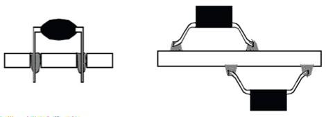
Figure 1: Through-hole (left) and surface-mount (right) connections on a PCB
Because saving board space and optimizing density/volume are such common motivators for product development, many designs include multiple boards that are either rigidly or flexibly connected to each other. This approach not only saves board real estate, it also allows for greater cost savings. For example, if a design contains a 256-pin ball grid array (BGA) processor requiring 10+ layers (which greatly drives PCB fabrication cost) but interfaces to many peripherals/connectors (that may require only two or four layers), a common way to save both space and cost is to separate them into two PCBs: one smaller, embedded PCB with 10+ layers and one secondary PCB with just four layers and most of the peripheral components (such as connectors). It’s common to mount “MCU PCBs” to “backplane PCBs” with high-density, high-pin–count board-to-board connections.
In the event that many satellite PCBs are required for things like displays and buttons, flexible connections can be used. Flex cabling, as it is often referred to, is common in LCD and motor connections and generally helps with tight-bending radii (which helps to keep things compact and low-profile) and physical stress associated with the assembly. The flex connection can either be a standalone cable that plugs into connectors or be directly fabricated with the PCB. Figure 2 shows a camera lens containing many (unpluggable) flex cable connections while Figure 3 demonstrates the differences of a “rigid flex” PCB with integrated flex cabling. While sometimes difficult to design and specify to a vendor, incorporating rigid-flex technology can greatly help save production costs and allow for a more reliable, tighter-fit design. However, assembly for rigid-flex can be more difficult due to the inability to physically separate two PCBs from each other.
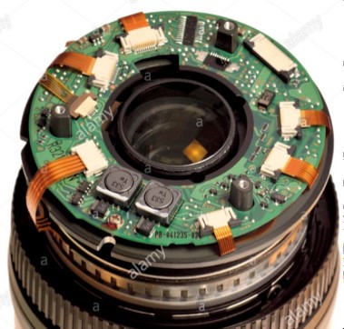
Figure 2: Camera lens assembly with flex cables
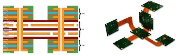
Figure 3: Rigid-flex PCB technology
Take into consideration the application to which the connectors will be applied
While on the topic of cabled connections, let’s quickly address some of the other important items to consider. One topic is ease of use, and the perfect example is a standard USB port. Over the years, USB connectors have improved in a variety of ways, including current-carrying capacity, signal density, and, with USB-C, a reversible, orientation-free connection. Conversely, orientation-dependent connectors that are keyed and only allow one-way (such as the classic USB 2.0 connectors) help guide the user and prevent misconnections. Locked connections typically provide better mechanical support and can require a plug to be turned (BNC connectors) or a tab to be squeezed (RJ-45 network cables). Basically, if a connector requires repeated usage, ease of use should certainly be at the top of the user’s requirements.
Some applications require high-speed, sensitive connections over longer distances, and this leads us to fiber optics. There are three main types of fiber optic connections: single mode, multimode, and plastic optical fiber (POF). A multimode connection allows for higher bandwidth but generally suffers in longer-distance applications due to its high dispersion and attenuation rate, making it ideal for shorter, LAN-based connections. Single-mode excels at longer distances and is great for applications such as RF broadband (your local cable company). Additionally, parallel data buses over connections such as peripheral component interconnect (PCI) are usually much faster than serial connections like USB (though USB-C allows for parallel connections as well). The speed and performance of the application will dictate how these interconnections are defined.
For some applications, such as aerospace and military, harsh operating conditions may end up driving the requirements. Some connectors feature special protections for electromagnetic interference (EMI), electrostatic discharge (ESD), vibration, and/or moisture. A common decision for designers is if a connector should be shielded or not. A shielded connector (covered by some conductive metal and may include an EMI gasket) may offer additional levels of protection against unwanted radiation and local magnetic fields but will usually be more bulky or expensive when compared with unshielded alternatives. Connectors with shells and corresponding pins can be grounded to assist with ESD introduced by human touch or other local sources of transients. Some connectors even contain shock-absorbing contacts to help with high-shock and high-reliability applications. Finally, connections that require protection against outside moisture often contain (or allow for) a seal. Figure 4 demonstrates all four of these variations in commonly occurring connections.

Figure 4: (L–R) Shielded DC power jack, shielded/grounded RJ-45 jack, vibration-resistant board-to-board connector, and waterproof USB connector
For high-load applications, selecting a connector with maximum current or voltage ratings can wind up driving the design process as well. Some connectors contain a mixed-signal pinout to support both data and power connections. Typically, the power pins have more capacity for current and may be a bit thicker, helping to prevent two separate power and data connectors/cables.
AC-voltage applications can also drive the selection of a connector and require a minimum clearance or separation between each pin (depending on the maximum voltage). This helps prevent against arcing, something that can be harmful for both the system and operator. Connectors will always list power ratings, and it’s important to follow these specifications during design while building in a healthy margin.
Lastly, sometimes the best (and least costly) solution is to design out the connector altogether and simply use exposed copper pads for a spring-loaded interface. While also providing a lower-profile footprint, it can help reduce component cost and allow for easier probing (based on flexibility of PCB location). Among of the most common applications are programming or testing interfaces. Embedded designs often include debug or programming ports, but why have a connector there if it isn’t normally used (and needed only for production or service)? Cable technology such as that of Tag-Connect (shown in Figure 5) allows for a lower-profile, lower-cost solution. While often used only as test points, consider using an array of pads for pogo-pin–based connections as well.
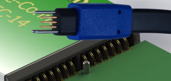
Figure 5: Tag-Connect’s pogo-pin cable technology
PCB Design Suites Can Help
Many CAD programs these days feature 3D visualization and mechanical file import/export support. One example is Solidworks Electrical (SWE). While traditionally a mechanical design CAD program, an electrical suite for Solidworks exists for easy integration with schematically defined PCBs and associated connections. The designer’s benefits include electrical design tools to help define interconnections and produce cable specifications, wiring diagrams, and even files that can be used in other PCB design programs to help with netlists while providing a full visualization of a systems’ interconnections. While many PCB-design programs contain 3D visualization features, some allow for file interchangeability to help define PCB shapes (via 2D files) and import component footprints (via 3D files), which can greatly help with checking against interferences and optimizing connector location.
Conclusion
Designing for PCB connections is entirely dependent on the application, and it generally starts with the user requirements, considering the design requirements, and figuring out if any special features are necessary. Often forgotten, the manufacturing requirements must also be considered so as to ensure that it can be fabricated and assembled with reasonable ease and cost.
PCB design suites of all shapes and sizes contain mechanical-related features that can significantly help lower the risk of design iterations and optimizing connector placement.