


Researchers in the US and Saudi Arabia are the first to have observed negative transconductance (NTC) inside multilayer molybdenum-disulphide (MoS2) transistors with optimized graphene/metal hybrid contacts. The NTC behaviour comes about thanks to competition between inter-layer charge transport and charges transport through a vertical potential barrier in the MoS2. This unique effect could be exploited for making frequency doublers and phase-shift keying circuits with only one multilayer transistor – something that would greatly simplify circuit design compared to conventional technology, says the team.
NTC devices are promising for low-power logical circuits, memories, oscillating and high-speed switching applications. In a typical n-type NTC transistor, the output current decreases with increasing gate voltage. It increases with increasing gate voltage in a p-type NTC device.


 Previous NTC devices were found to work by either quantum-mechanical tunnelling or thanks to charge mobilities degrading at high electrical fields. A team of researchers led by Xiangfeng Duan of the University of California at Los Angeles (UCLA) has now discovered a third possible mechanism by investigating the charge transport in multilayer 2D semiconductors (2DSCs) made from MoS2 containing optimized van der Waals contacts.
MoS2 belongs to the family of single-layer transition-metal dichalcogenides (TMDs). These are quasi-two-dimensional materials with the chemical formula MX2, consisting of an atomic plane of a transition metal M (Ti, Nb, Mo, Re) sandwiched between the atomic planes of a chalcogen X (S, Se or Te). These materials go from being indirect bandgap semiconductors in the bulk to direct bandgap semiconductors when scaled down to monolayer thickness. These monolayers efficiently absorb and emit light and so might find use in a variety of electronic and optoelectronic device applications.
TMDs also boast good carrier mobilities as well as other attributes such as coupled spin-valley physics and the valley Hall effect, which could be put to good use in devices like transistors, memories, logic circuits, light-emitting diodes and photodetectors.
Graphene as an optimized van der Waals contact
Until now, most studies of 2D semiconductors focused on lateral intra-layer charge-transport properties. Studying vertical inter-layer transport in these materials was more difficult because of un-optimized contacts in which a finite Schottky barrier dominates carrier transport because of Fermi-level pinning of charges at the metal–2DSC interface.
Duan and colleagues have now employed graphene as an optimized van der Waals contact in 2D MoS2 for the first time and have found that the built-in potential barrier inside this material can influence vertical charge transport to produce NTC behaviour. The barrier forms near the substrate on which the MoS2 layers have been grown and extends to the bulk region thanks to different doping mechanisms and inhomogeneous carrier distributions, say the researchers. This is very different to the situation in conventional semiconductors with their homogenous doping from bulk dopants.
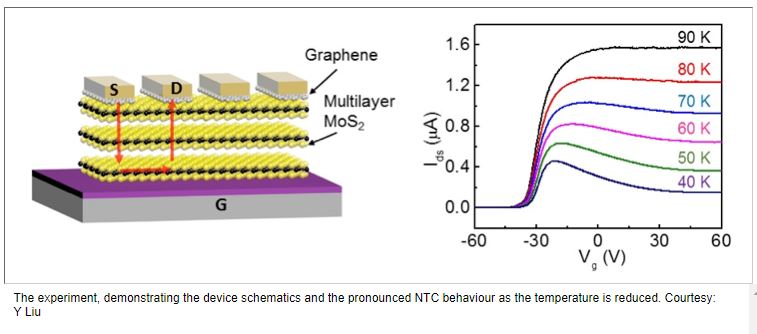
“We observed this novel phenomenon in back-gated MoS2transistors with a new metal/graphene hybrid contact (see figure),” explains team member and lead author of the study Yuan Liu. “To make the device, we first mechanically exfoliated MoS2 flakes onto a silicon substrate with 300 m silicon oxide. Next, we pre-patterned monolayer graphene (grown by chemical vapour deposition) into stripe arrays using photolithography and oxygen plasma and transferred these on top of the MoS2 flakes. Finally, we defined and deposited a thin layer of Ni/Au on top of graphene as electrodes using e-beam lithography and e-beam evaporation.”
Reducing the Fermi-level pinning effect
The graphene/metal hybrid contact greatly reduces the Fermi-level pinning effect and the contact barrier, thus allowing for an optimized contact, he told nanotechweb.org. We are thus able to observe NTC transport in MoS2 – something that is impossible in devices with a larger contact barrier.
“Our results suggest that inter-layer charge transport and transport through the vertical potential barrier are important in 2DSCs,” he adds. “These mechanisms were largely overlooked in previous studies. What’s more, when the temperature is decreased, the vertical barrier becomes even more pronounced and begins to compete with lateral in-plane transport.”
The finding could help in the development of simple oscillating or phase-shifting circuits made from just one type of multilayer transistor (rather than both n- and p-type ones), so greatly simplifying circuit design. And since the device is limited to relatively low working temperatures (of less than 100 K), it may come in useful in space technology and satellite-communication applications where low temperatures are the norm.
Duan and colleagues say they are now busy looking into the origins of the doping mechanism in 2DSCs. “We hope to be able to control the surface-doping and vertical-potential barrier in these materials using different substrates and contact electrodes,” reveals Liu.
Author: Belle Dumé
Article Courtesy: nanotechweb.org