


In recent years, resonant converters have become more popular and are widely applied in various applications like server, telecom, lighting and consumer electronics. One key attractive characteristic is that a resonant converter can easily achieve high efficiency and
allow high frequency operation with their intrinsic wide softs witching ranges. This paper highlight the 300W power supply featuring digital control of half bridge LCC resonant converter along with synchronous rectification.

Technical Marketing Manager – Power & Energy, SRA System Research and Applications, STMicroelectronics
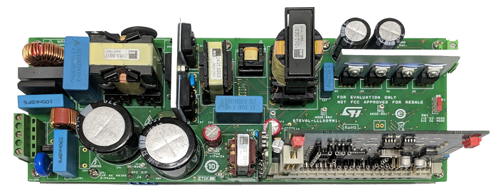
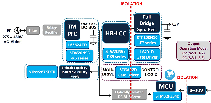
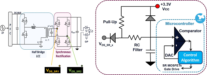
The STEVAL–LLL009V1 shown in Figure 1, is a digitally controlled 300W power supply. The primary side constitutes of PFC and DC-DC power stage (half bridge LCC resonant converter) while the secondary side constitutes synchronous rectification and STM32F334 microcontroller. The DC-DC power stage (half bridge LCC resonant converter) and output synchronous rectification are controlled digitally using STM32F334 microcontroller, while the power factor correction (PFC) stage works in transition mode based on L6562ATD.


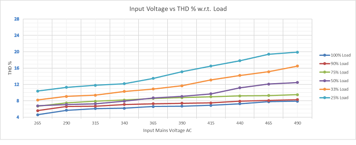
The evaluation kit can either work in constant voltage (CV) mode or constant current (CC) mode as per requirement. The on-board fast protection circuits guarantee all essential protection features with high reliability. The performance of the evaluation kit developed has been evaluated under AC mains ranging from (270-480V) over the entire range of load. The power quality parameters are within the acceptable limits of harmonic standard IEC 61000-3- 2.

Staff Engineer, SRA System Research and Application, STMicroelectronics
INTRODUCTION
The proposed solution adopts a digital conversion control approach rather than the standard design based on analog ICs. The main advantage of the digital control is programming flexibility to tune the parameters and the operating points on the fly, for any given condition, without any HW modification, whereas the analog control can only be tuned for a specific range. Advanced features such as dimming methods (analog or digital), dimming controls (0- 10V, Wireless communication), dimming resolution, temperature
monitoring, various protections, and communication functions tend to be significantly more cost-effective since they can be implemented by a single IC and are easier to implement using digital techniques compared to analog control. Additionally, the digital control guarantees more stability than analog in noisy conditions: a solution digitally controlled is less sensitive to component tolerance, temperature variations, and voltage drift.
SYSTEM OVERVIEW
The STEVAL-LLL009V1 evaluation kit converts 270 V to 480 V AC mains input voltage to 48 V DC, 6.25 A maximum current in a constant voltage (CV) mode while in constant current (CC) mode it can deliver 6.25 A of current with an output voltage ranging from 36 – 48V. The evaluation kit can either be configured in CV mode or CC mode by using the toggle switch SW1 mounted on the main power board.
The DC-DC power stage is referred to as the primary ground while the microcontroller is referred to as the secondary ground. Thanks to STGAP2DM galvanically isolated half bridge gate driver which drives the DC-DC power stage MOSFETs with the control signal coming from the microcontroller.
Figure 2 present the block diagram of the STEVAL-LLL009V1 evaluation kit which embeds the topologies and components being used for different sections.
On evaluation kit, there is a provision of 0-10V input to control the brightness of the LEDs. The dimming control 0-10V is only applicable when the evaluation kit is operated in constant current (CC) mode. The analog dimming approach is implemented in STEVAL-LLL009V1 evaluation kit with a current resolution of 1%.
A daughter card with an isolated amplifier serves the purpose of sensing of PFC output voltage that is also the input voltage to the DC-DC power stage.
The PFC stage is based on MDmeshTM K5 Power MOSFET while the half bridge of the LCC converter is based on MDmeshTM DK5 Power MOSFETs for high efficiency performance. Synchronous rectification (SR) with STripFETTM F7 Power MOSFETs is employed on the secondary side to reduce conduction losses.
The evaluation kit is equipped with comprehensive safety provisions like open circuit, short circuit, resonant current protection, DC-DC power stage input under voltage and over voltage protection.
Both the primary and secondary sections are supplied by an off-line flyback circuit based on VIPer267KDTR which provides regulated voltages to the control board, the gate driver ICs and the signal conditioning circuits.
The experimental results show high efficiency, power factor near unity, and low THD% under wide input voltage and load conditions due to the performance of the ST power products as well as the control strategies implemented using the 32-bit STM32F334 microcontroller.
LCC ResoNANT CONVERTER
The DC-DC power stage converts the PFC output voltage to the desired output voltage. There are various topologies which can be used for DC-DC conversion especially LLC resonant converter and LCC resonant converter etc. Each topology has its own advantages and disadvantages. The applications like battery chargers and LED lighting may require their isolated DC-DC power stages to handle wide input or output voltage ranges. Considering the requirements, the half bridge LCC resonant topology is implemented in DC-DC power stage of STEVAL-LLL009V1 as shown in Figure 3.
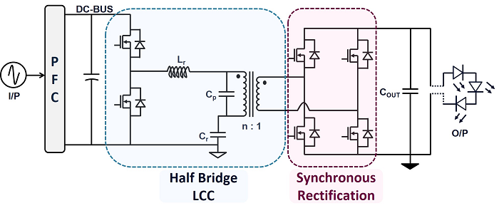
In STEVAL-LLL009V1 the parallel capacitor Cp is connected to the secondary of the transformer. As a result, the parasitic capacitances of the synchronous rectification and the leakage inductance of the transformer becomes a part of the resonant tank.
The PFC output voltage charges the bulk capacitor, in order to generate a stable DC-BUS. The half bridge configuration MOSFETs switches to generate a square voltage waveform between GND and DC-BUS. The square voltage is applied to the LCC resonant tank circuit which comprises of capacitor Cr, capacitor Cp (placed in secondary), inductor Lr and isolation transformer.
The half bridge of the LCC resonant converter high voltage MOSFETs/switches are driven with 50 percent PWM duty cycle and an appropriate dead time. As the approximately sinusoidal resonant tank current always lags the voltage waveform (inductive region) as shown in Figure 4, the MOSFET output capacitance has time to discharge during the dead time before the next turn-on, and achieve zero voltage switching (ZVS). PWM switching frequency control is used to regulate the voltage gain of the resonant tank and keep the converter in the inductive region. This allows ZVS over the entire operating range and reduced switching losses.
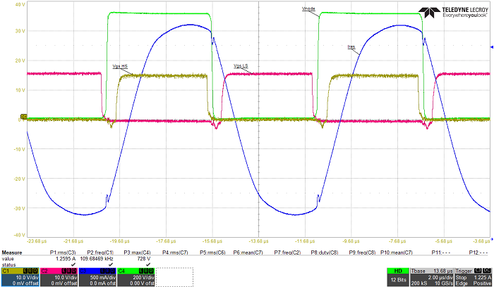
Table 1: LCC vs LLC Resonant Converter
| Resonant Converter | LCC Converter | LLC Converter | |
| fr1 | |||
| fr2 | |||
| Desired Operating Region | foperation > fr2 | fr1 < foperation < fr2 | |
| Key Features | LCC has narrower frequency variation.
May not need bursting at light load. |
LLC has lower RMS current than LCC.
Better efficiency on LLC w.r.t. LCC. |
|
| Block Diagram | |||
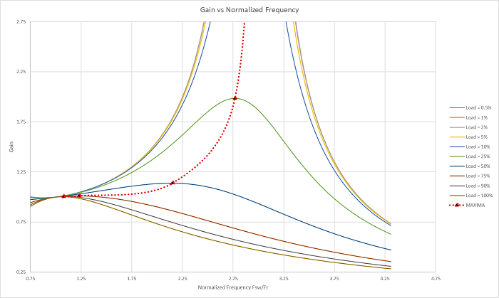
The gain of the half bridge LCC resonant converter in the evaluation kit has been analyzed using the fundamental harmonic analysis (FHA) method.
Based on the gain equation derived using FHA method and the LCC parameters selected for half bridge LCC resonant converter in STEVAL-LLL009V1 evaluation kit, the plot between gain and normalized is shown in Figure 5.
SYNCHRONOUS RECTIFICATION (SR)
On the secondary side of the transformer shown in Figure 3, the input voltage waveform is rectified by the synchronous rectifier in full bridge configuration and smoothed by output capacitors. The synchronous rectification stage is controlled digitally by the STM32F334 microcontroller.
Synchronous rectification (SR) stage node voltages (VDS_SR1 and VDS_SR2) are sensed to drive SR stage MOSFETs. The MOSFET VDS (Drain-Source voltage) sensing and the control algorithm is explained below.
The sensing network is composed of a fast diode and a pull-up resistor connected to the microcontroller (MCU) supply voltage as shown in Figure 6. When the SR MOSFET drain voltage is above the MCU Vcc, the diode is reverse biased and the sensed voltage is pulled up to Vcc. When drain voltage is below Vcc, the diode is forward biased and the sensed voltage is equal to this voltage plus the voltage drop of the diode that gives a positive shift. The current during positive biasing is limited by the pull-up resistor.
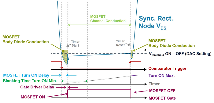
Initially the body diode of SR MOSFETs start conducting and VDS is sensed. Thanks to the VDS sensing technique implemented, when the voltage (VDS) falls below the set threshold (Vthreshold_ON – OFF set by MCU DAC peripheral), the comparator output (falling edge) triggers the MCU TIMER peripheral in one pulse non-retriggerable mode as shown in Figure 7.
The MCU TIMER peripheral initiates a pulse to corresponding synchronous rectification gate driver. The pulse sustains for a certain minimum time (TON min).
When the voltage (VDS) increases above the set threshold (Vthreshold_ON – OFF set by MCU DAC peripheral), the comparator output (rising edge) resets the MCU TIMER peripherals and correspondingly the pulse is stopped at the corresponding synchronous rectification gate driver as shown in Figure 7.
The MCU continuously monitors the DC-DC power stage (HB-LCC) frequency and the output current. In case the frequency exceeds above set threshold with hysteresis or the output current falls below set threshold with hysteresis, the microcontroller (MCU) disable the gate drive to synchronous rectification stage. Thanks to MOSFETs body diode for rectification at this stage. The synchronous rectification gate drive gets enabled when the frequency falls below set threshold with hysteresis or the output current rises above set threshold with hysteresis.
Depending on the DC-DC power stage (HB-LCC) operating frequency, the threshold (Vthreshold_ON – OFF) is being adjusted from the look-up table stored in MCU.
Experimental RESULTS
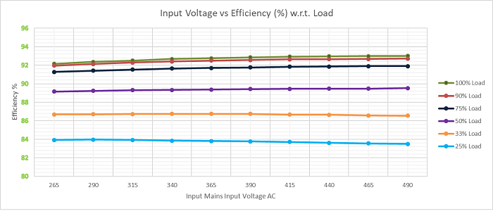
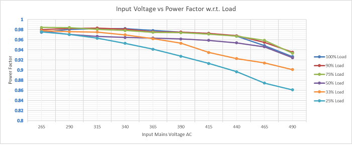
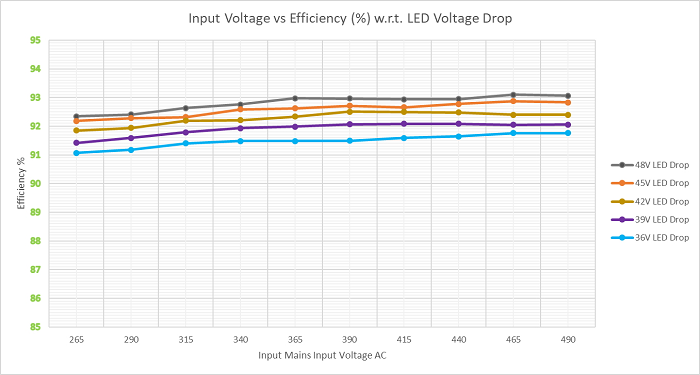
The overall Efficiency, Power Factor (PF), and Total Harmonic Distortion (THD) of the STEVAL-LLL009V1 has been calculated at different loads. With 100% load, the efficiency is above 93.5%.
Figures 8, 9, 10 and 11 show the evaluation kit performance in terms both in constant voltage (CV) and constant current (CC) configuration.
The digitally controlled power supply presented in the current work can deliver the power output of 300W both in constant voltage (CV) and constant current (CC) mode. The experimental results show high efficiency, power factor near unity, and low THD% under wide input voltage and load conditions due to the performance of the ST power products as well as the control strategies implemented using the 32-bit STM32F334 microcontroller. For more details, please contact STMicroelectronics sales office.
For more information, visit www.st.com