The need to step down high bus voltages to lower voltages to power ICs and other loads is growing across a variety of systems including automotive, industrial automation, telecommunications, computing, white goods, and consumer electronics. The challenge for designers is to execute this down-conversion with maximum efficiency, minimal thermal loading, at low cost, and with the smallest possible solution size.
Conventional asynchronous buck converters offer a potentially low-cost solution, but also have lower conversion efficiencies that don’t meet the needs of many electronic systems. Designers can turn to synchronous DC/DC converters and synchronous DC/DC controllers to develop compact solutions that deliver high efficiencies.


This article briefly describes the performance requirements of electronic systems for high-efficiency DC/DC conversion and reviews the difference between asynchronous and synchronous DC/DC converters. It then introduces several synchronous DC/DC converter design options from Diodes, Inc., STMicroelectronics, and ON Semiconductor along with evaluation boards and design guidance that can jump-start development of high-efficiency solutions.
Why synchronous DC/DC converters are needed
The growing requirements for higher efficiency in all types of electronic systems combined with increasing system complexities is resulting in a corresponding evolution of power system architectures and power conversion topologies. With a growing number of independent voltage domains to support increasing functionality, distributed power architectures (DPAs) are being used in more and more electronic systems.
Instead of having several isolated supplies to drive the various loads, a DPA has one isolated AC/DC power supply that produces a relatively high distribution voltage, and multiple, smaller buck converters that down convert the distribution voltage to a lower one as required by each individual load (Figure 1). The use of multiple buck converters offers the advantages of smaller size, higher efficiency, and better performance.
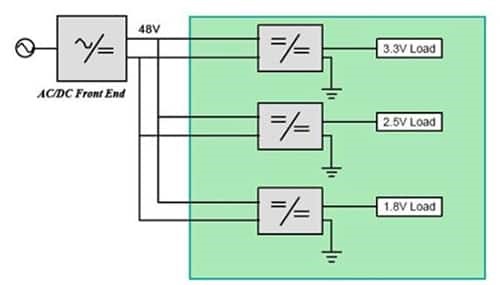 Figure 1: Distributed power architecture showing the main isolated AC/DC power supply (front end) and the multiple non-isolated DC/DC converters powering low voltage loads. (Image source: Digi-Key Electronics)
The process of selecting between asynchronous and synchronous buck converters is based on the tradeoffs between cost and efficiency. If a lowest solution cost is required and lower efficiency and higher thermal loading can be accepted, an asynchronous buck solution may be preferred. On the other hand, if efficiency is the priority and a cooler running solution is preferred, a higher cost synchronous buck converter is generally the superior choice.
Synchronous vs. asynchronous buck converters
A typical asynchronous buck converter application is shown in Figure 2. The LM2595 from ON Semiconductor is a monolithic integrated circuit that includes the main power switch and the control circuitry. It is internally compensated to minimize the number of external components and simplify the power supply design. It delivers a typical conversion efficiency of 81% and dissipates 19% of the power as heat, while a synchronous buck solution will have a typical conversion efficiency of about 90%, dissipating only 10% of the power as heat. That means that the thermal losses in an asynchronous buck converter are nearly twice as large as the thermal losses in a synchronous buck converter. Therefore, the use of a synchronous buck converter greatly simplifies thermal management challenges by reducing the amount of heat generated.
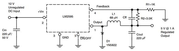 Figure 2: Typical asynchronous buck converter application showing the output rectifier (D1), the output filter (L1 and Cout), and the feedback network (Cff, R1 and R2). (Image source: ON Semiconductor)
In a synchronous buck converter, such as the ST1PS01 from STMicroelectronics, the output rectifier is replaced by synchronous MOSFET rectification (Figure 3). The lower “on” resistance of the synchronous MOSFET compared with the output rectifier in an asynchronous buck converter reduces losses and results in significantly higher conversion efficiencies. The synchronous MOSFET is internal to the IC, eliminating the need for an external rectifier diode.
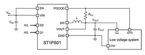 Figure 3: Synchronous buck application circuit showing the elimination of the external output rectifier diode. Output filtering and feedback components are still required. (Image source: STMicroelectronics)
There is a cost for the higher efficiency and lower thermal loading made possible with a synchronous buck converter. With a single power switching MOSFET and a diode for rectification, asynchronous buck converter controllers are much simpler (and smaller) since they do not have to deal with the possibility of cross-conduction or “shoot-through”, and there is no synchronous FET to control. A synchronous buck topology requires a more complicated driver and anti-cross conduction circuitry to control both switches (Figure 4). Ensuring that both MOSFETs don’t turn on at the same time and create a direct short requires more complexity and results in larger and more expensive ICs.
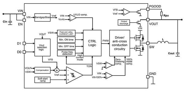 Figure 4: Synchronous buck converter IC block diagram showing the two integrated MOSFETs (next to the pin marked ‘SW’) and the added Driver/anti-cross conduction circuitry. (Image source: STMicroelectronics)
Although pulse width modulation controlled synchronous buck converters are more efficient under moderate or full load conditions, asynchronous buck converters often deliver higher conversion efficiencies under light load conditions. That, however, is becoming less and less the case as the latest synchronous buck converter implementations include multiple operating modes that enable designers to optimize low load efficiencies.
Synchronous buck for 5 volt and 12 volt power distribution
For designers using 5 and 12 volt power distribution in consumer products and white goods, Diodes, Inc. offers the AP62600, a 6 ampere (A) synchronous buck converter with a wide input range of 4.5 to 18 volts. The device integrates a 36 milliohm (mΩ) high-side power MOSFET and a 14 mΩ low-side power MOSFET to provide high-efficiency step-down DC/DC conversion.
The AP62600 needs minimal external components as a result of its constant on-time (COT) control. It also delivers a fast transient response, easy loop stabilization, and low output voltage ripple. The AP62600 design is optimized for electromagnetic interference (EMI) reduction. The device has a proprietary gate driver scheme to resist switching node ringing without sacrificing MOSFET turn-on and turn-off times, which reduces high-frequency radiated EMI noise caused by MOSFET switching. The device is available in a V-QFN2030-12 (Type A) package.
There is a power-good indicator which alerts users to any fault conditions that may arise. A programmable soft-startup mode controls inrush current at power-up, enabling designers to implement power sequencing when using multiple AP62600s to supply large integrated devices, such as field programmable gate arrays (FPGAs), application specific ICs (ASICs), digital signal processors (DSPs), and microprocessor units (MPUs).
The AP62600 gives designers a choice of three operation modes to meet the specific needs of individual applications (Figure 5). High efficiency can be realized across all loads with pulsed frequency modulation (PFM) operation. Other modes available include pulse width modulation (PWM) to get the best ripple performance, and an ultrasonic mode (USM) which avoids audible noise at light loads.
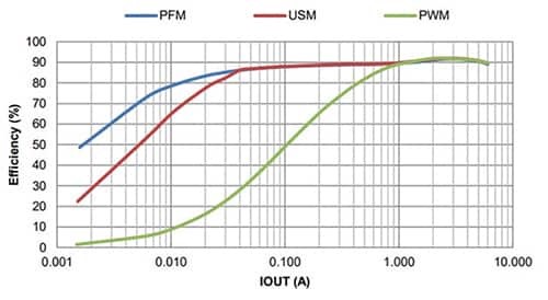 Figure 5: The AP62600 gives designers a choice of three operation modes to meet the needs of individual applications: PFM, USM, and PWM. (Image source: Diodes, Inc.)
To help designers start using the AP62600, Diodes, Inc. offers the AP62600SJ-EVM evaluation board (Figure 6). The AP62600SJ-EVM has a simple layout and allows access to the appropriate signals through test points.
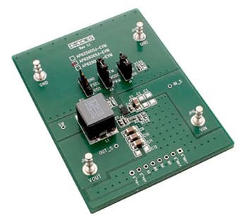 Figure 6: The AP62600SJ-EVM evaluation board provides a simple and convenient evaluation environment for the AP62600. (Image source: Digi-Key Electronics)
Synchronous buck for 24 volt buses
The L6983CQTR from STMicroelectronics features a 3.5 to 38 volt input range and delivers up to 3 A of output current. Designers can use the L6983 in a wide range of applications, including 24 volt industrial power systems, 24 volt battery-powered equipment, decentralized intelligent nodes, sensors, and always-on and low-noise applications.
The L6983 is based on a peak current mode architecture with internal compensation and is packaged in a 3 mm x 3mm QFN16, thereby minimizing design complexity and size. The L6983 is available both in low consumption mode (LCM) and low noise mode (LNM) versions. LCM maximizes the efficiency at light loads with controlled output voltage ripple, making the device suitable for battery-powered applications. LNM makes the switching frequency constant and minimizes the output voltage ripple for light load operations, meeting the specification for noise sensitive applications. The L6983 allows the switching frequency to be selected in the 200 kilohertz (kHz) to 2.3 megahertz (MHz) range with optional spread spectrum for improved EMC.
STMicroelectronics offers the STEVAL-ISA209V1 evaluation board to enable designers to explore the capabilities of the L6983 synchronous monolithic step-down regulator and jump-start their designs.
Synchronous buck controller for computing and telecom designs
The NCP1034DR2G from ON Semiconductor is a high voltage PWM controller designed for high performance synchronous buck DC/DC applications with input voltages up to 100 volts. This device is designed for use in 48 volt non-isolated power conversion in embedded telecommunications, networking and computing applications. The NCP1034 drives a pair of external N−channel MOSFETs as shown in Figure 7.
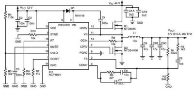 Figure 7: Typical application circuit for the NCP1036 synchronous buck controller IC showing the high-side and low-side MOSFETS (Q1 and Q2, respectively). (Image source: ON Semiconductor)
The NCP1036 features a programmable switching frequency from 25 kHz to 500 kHz and a synchronization pin that allows the switching frequency to be externally controlled. Providing both these frequency controls enables designers to select the optimal value for each specific application and to synchronize the operation of multiple NCP1034 controllers. The device also includes user programmable undervoltage lockout and hiccup current limit protection. For low voltage designs, an internally trimmed 1.25 volt reference voltage can be used for more precise output voltage regulation.
Four undervoltage lock-out circuits are included to protect both the device and the system. Three are dedicated to specific functions; two protect the external high-side and low-side drivers, and one protects the IC from starting prematurely before VCC is under a set threshold. The fourth undervoltage lock-out circuit can be programmed by the designer using an external resistor divider: as long as VCC is below the user set threshold value, the controller remains off.
To help designers get started using the NCP1034, ON Semiconductor offers the NCP1034BCK5VGEVB evaluation board (Figure 8). This eval board was designed with several options to support a variety of system needs. There is a linear regulator powering the IC, and the designer can choose whether it does so using either a Zener diode or a high voltage transistor by selecting the appropriate resistor. Designers also have a choice of second type (voltage-mode) compensation or third type (current-mode) compensation, selectable ceramic or electrolytic output capacitors, and various input capacitance values. There are two header pins: one for easy connection to an external synchronization pulse source to allow the board to connect directly to the other NCP1034 demo board; the other to connect to the SS/SD pin that can be used to shut down the controller by connecting it to ground.
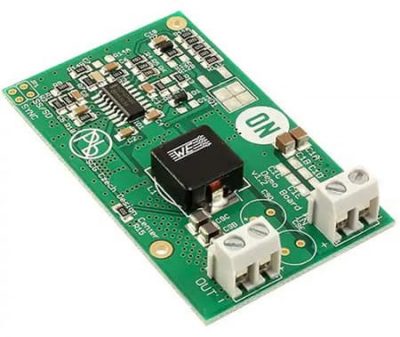 Figure 8: The NCP1034BCK5VGEVB eval board includes multiple options to help designers quickly start new designs. (Image source: Digi-Key Electronics)
Conclusion
The need to step down high bus voltages to lower voltages to power ICs and other loads is increasingly required across a variety of systems including automotive, industrial automation, telecommunications, computing, white goods, and consumer electronics.
As shown, designers can turn to synchronous buck power converters to implement this down-conversion with maximum efficiency, minimal thermal loading, at low cost, and with the smallest possible solution size.