

Researchers at Oak Ridge National Laboratory and Korea’s Sungkyunkwan University are using advanced microscopy to nanoengineer promising materials for computing and electronics in a beyond-Moore era.
Historically, computers have become faster and more powerful by Moore’s Law, an observation that technology advances as transistor sizes shrink. Today’s nanometer-scale transistors are reaching practical limits and new approaches are needed to scale existing technology.


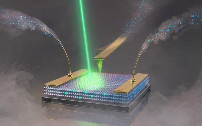
A team at ORNL’s Center for Nanophase Materials Sciences has applied a focused beam of helium ions to locally tailor ferroelectricity in a metal oxide thin film, enhancing a useful property for transistors and memory. Results show how light ion microscopy can unlock unique functionalities in materials and create new pathways to design future devices.
“This project highlights the advanced ion beam and scanning probe capabilities available to CNMS users, which open new frontiers to locally control and understand materials properties on the nanoscale,” said ORNL’s Liam Collins.