

, instead of side by side, allows for space savings and transistor scaling. However, this architecture causes new fabrication challenges that need to be overcome. The image displays")
Computing power has experienced exponential growth over the last 70 years. This has largely been achieved through transistor scaling. Due to a continuous reduction in the size of transistors, engineers have been able to pack more and more of them onto a single chip. This has led to faster, more powerful, and more energy-efficient devices. Improvements in fabrication processes and materials, along with better circuit design techniques, have enabled this scaling.
As transistors have become smaller and more densely packed, we have started to reach limitations caused by the laws of physics. Short channel effects have hindered the downscaling in the size of transistors. Leakage currents due to quantum effects have also hampered the switching ability of smaller transistors. Excessive heat density is another challenge that has become more important as transistor dimensions have approached atomic scale.


To mitigate these challenges, researchers have developed new 3D transistor architectures that don’t rely on traditional planar designs. These designs seek to improve performance and reduce power consumption by taking advantage of a third dimension. FinFET and Gate-All-Around transistors are examples of this move towards 3D designs. These new 3D architectures have become prevalent in next generation transistor development.
In CMOS design, the NFET and PFET transistors have traditionally been fabricated next to each other. However, by stacking transistors vertically (Fig 1), it is possible to increase the density of devices on a chip, even if there’s no reduction in the size of the transistors or their components. This proposed architecture, referred to as a Complementary-Field Effect Transistor (CFET), has been well-described in technical literature.
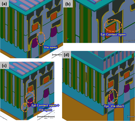
windows during manufacturing. Failure
to adhere to these windows leads to unintended
opens and shorts. Various failure modes are
shown above (a) Failure of the Via to reach the
layer below causes a via open
CFET fabrication requires new schemes for metal wiring and the power rails used to power the device. The CFET architecture is an evolution of a Gate-All-Around (GAA) architecture, where the NFET and PFET are stacked vertically rather than side by side.
Two CFET manufacturing integration schemes have been proposed – one that grows the PFET and NFET together in a monolithic manner and the other that grows them sequentially. The monolithic approach offers better performance and lower cost. However, extremely high aspect ratio (HAR) etching is needed for monolithic integration. The sequential approach allows more flexibility in NFET and PFET channel materials. However, a very accurate NFET-PFET alignment is needed using sequential integration. Additionally, thermal budget is also a concern.
In either scheme, very tight parameter windows exist for the fabrication process steps. Failure to adhere to these tolerance windows causes unintended shorts and opens. Fig 2 highlights a few examples of potential CFET device failures (images generated using SEMulator3D).
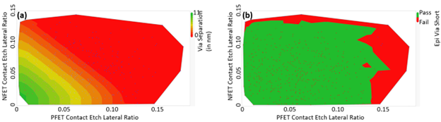
The high aspect ratio etch process required during CFET fabrication is difficult to perform. The lateral ratio (a parameter that measures how directional an etch is – lower means more directional or anisotropic; higher means isotropic) of these etch steps must be kept low and within a small tolerance window.
To study problems with this, etch process, we performed a virtual 500 trial DOE (design of experiment) using SEMulator3D. Fig. 3 displays the results of the experiment. Metrology measurement points were included in the simulation to measure the minimum distance between the NFET and PFET contact vias after the virtual etch process was completed. A higher separation between the vias is desirable. Fig 3(a) shows the small tolerance window of the etch lateral ratios in order to have a minimum distance between the vias that is within specification (via separation >= 5 nm). Fig 3(b) highlights the regions where the model predicted that there would be a short between the Source/Drain Epi and a neighbouring via (failure shown in red).
SEMulator3D modeling software has virtual DOE capabilities that can help us establish key process parameters and their tolerance windows. Reliable fabrication processes need to be developed to mitigate CFET failure modes. There are still many challenges to be overcome before CFET designs become mainstream, but this new architecture represents a promising new direction for the future of computing.