


Silicon carbide (SiC) and gallium nitride (GaN) are two semiconductor materials that are creating a significant shift in the power electronics market.
The majority of electronics today rely on metal oxide semiconductor field effect transistors (MOSFETs), which were invented in 1959 at Bell Labs and widely adopted during the early 1960s. MOSFETs control the electrical conductivity of a device, converting energy to power. The ability to change conductivity through the amount of applied voltage is the means used for amplifying or switching electronic signals.


The building block of MOSFETs since their inception has been silicon, but performance limits have been reached for this material. Increasing requirements for energy efficiency, power density and environmental pollution concerns has created the need for new types of materials used in power switching technology. Silicon carbide and gallium nitride are two innovative materials delivering key benefits to the semiconductor industry that include better efficiency, improved performance and reduced costs.
A recent study by Gartner reports that SiC and GaN technologies in transistors are having significant impacts on strong growth markets:
- Electric vehicles (EV) and transportation: Efficiency improvements result in lower battery costs and more miles per charge. ST Microelectronics cites that SiC technology delivers a 20% improvement in miles per charge as well as reduced battery costs.
- EV charging infrastructure: Greater power delivery and the reduction of charging time by more than half delivers much better results than what is achievable by today’s silicon solutions.
- Renewable energy: SiC transistors halve power loss, directly lowering cost of energy generation. In addition, Infineon Technologies quotes a 20% reduction in system costs due to thermal design simplifications.
- Industrial power supplies: Up to 10% efficiency improvements in kW power supplies provide for compelling opex improvements — lower runtime and maintenance.
- 5G and communications: GaN has higher bandwidth and power density compared to alternatives, critical for global 5G development and deployment.
The advantages of SiC, GaN over traditional Si
Energy usage and its conversion from source to final application have been a continuous subject of development since the invention of the wheel. Today, we think more about electrical energy and power conversion from a generator output to an end-voltage for a host of applications, be it 0.6VDC for a processor, 24VDC to 500VAC for an industrial motor drive or 400VDC to charge an EV battery.
The conversion process invariably uses power semiconductor switches and silicon-based types have been dominant for decades in the form of Si-MOSFETs and insulated-gate bipolar transistor (IGBTs). Power loss in silicon switches is a major factor in system inefficiency.
SiC and GaN have characteristics that enable noticeable improvements in power conversion efficiency. These wide band-gap (WBG) devices are not a simple substitution for Si though and application circuits must be designed to match, especially if the full performance benefits are to be extracted.
Figure 1 demonstrates the key differences between the materials.
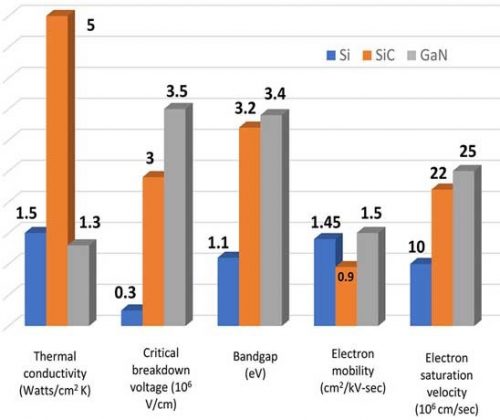
Figure 1: Key differences between Si, SiC and GaN materials
Si, SiC and GaN – conduction losses
Si-IGBTs have a minimum on-state collector-emitter saturation voltage that with collector current sets conduction losses. Si-MOSFETS have an on-state resistance so that power dissipated is I.R(ON)2 (noted as: i2 * Ron) which can be prohibitive at high current levels. At low voltage and low to medium power, Si-MOSFETs with low R(ON) can have less conduction loss than IGBTs. SiC and GaN devices have a much higher critical breakdown voltage than Si, allowing for a thinner drift layer and higher doping concentration. This leads to lower on-resistance for a given die area and voltage rating, providing for greater efficiency through reduced power loss. Additionally, SiC has a thermal conductivity more than three times better than Si, enabling the use of smaller die for the same temperature rise. SiC and GaN also provide efficiency improvements over Si by having higher maximum operating temperatures, limiting stress.
Si, SiC and GaN – switching losses
High converter switching frequency is a desirable characteristic because associated components, particularly magnetics, can be smaller, yielding miniaturization benefits and cost savings. However, switching losses in all devices scale directly with frequency. IGBTs are rarely operated above 20kHz because of power loss due to ’tail current,’ necessary snubbers and charge / discharge of high device capacitances. Si-MOSFETs can switch at hundreds of kHz but energy lost, energy stored in output capacitance (EOSS), in circulating current to the output capacitance becomes a limiting factor as frequency rises. SiC and GaN deliver much higher electron saturation velocity and much lower capacitances, providing substantial benefits in higher speed switching and decreased power loss.
The characteristics of devices in the ’third quadrant‘ are also of importance. This is when the conducting channel is reverse biased and occurs in ’hard switching‘ applications when ’commutation‘ occurs in inverters. (See Figure 2.) IGBTs do not conduct in reverse so an anti-parallel diode is required, which must be a fast recovery type with a low voltage drop. Si- and SiC-MOSFETS have inherent fast body diodes but can conduct through their channels in reverse with low loss and no reverse recovery effect when switched ON via their gates.
’Dead time‘ is when the channel is reverse biased but not set to ON via the gate. This causes the body diode to conduct because of significant power loss caused by the relatively high forward voltage drop. GaN switches are configured as high electron mobility transistors (HEMTs) which have no body diode. Like MOSFETs, HEMT channels can conduct in reverse but there is also a body diode effect through the channel during any dead time. This produces a voltage drop approximately equal to the gate threshold voltage in the range of 2V. This can cause power dissipation unless the channel is actively turned ON.

Figure 2: A hard switched synchronous buck converter forces body diode D to conduct during ‘dead times.’
Practical implementation of SiC, GaN devices
Operating maximum voltages are important considerations for different switching technologies. The maximum voltage for high power Si-MOSFETs is around 950V, for GaN HEMTs it is 600V and for SiC MOSFETs around 1,700V. IGBTs are still preferred at very high voltages although MOSFETs can be stacked in some topologies to reduce voltage stress. When over-voltage does occur, IGBTs and MOSFETS have a protective avalanche mode with different device-dependent energy ratings. GaN HEMTs do not have an avalanche mode and therefore catastrophically fail under over-voltage stress. GaN device manufacturers must therefore ensure that a large safety margin exists between datasheet rated and absolute maximum voltages.
Optimum gate drive arrangements can vary greatly between device technologies. Silicon insulated-gate bipolar transistors (Si-IGBTs) have insulated gates but a high total gate charge. This requires significant drive power, scaling directly with gate voltage swing and frequency, so that the largest devices need several watts at realistic switching frequencies. Silicon metal-oxide-semiconductor field-effect transistors (Si-MOSFETs) have much lower gate charge and lower drive power requirements. Like IGBTs, Si-MOSFETs have a gate threshold voltage in the range of 10V for full enhancement. Absolute maximum gate voltage is typically +/-25V. The gate is often driven to a negative voltage, in the range of -12V, to switch the device OFF. This is to counter the effects of Miller capacitance and any common inductance in the source/emitter connection, both of which tend to produce transients which oppose the OFF-state gate drive. (See Figure 3.)
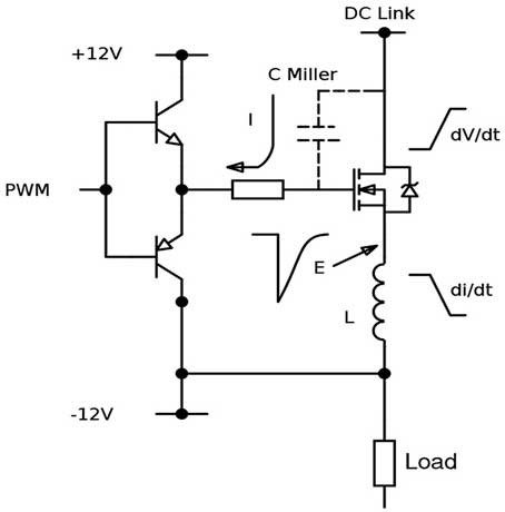
Figure 3: Negative gate drive counters effect of Miller capacitance and source inductance transients.
Compared to Si, SiC and GaN have extremely low total gate charge and insignificant drive power requirements. SiC gates must be driven to nearly 20V for full enhancement, close to the typical absolute maximum of +25V. Protection clamp diodes are often engineered into designs to avoid voltage stress. Gallium nitride high-electron-mobility transistors (GaN HEMTs) are current driven by voltage in the range of 3V, producing the few mA required to turn the device fully ON. The voltage varies greatly with temperature and drain current, so is not normally specified as a threshold voltage (VTH). A maximum gate current is therefore specified, measured in tens of mA, although amps of pulsed current are allowed dependent on pulse width and repetition rate.
Both SiC and GaN can experience ‘phantom’ turn ON due to the extremely high current rate-of-change (di/dt) and instantaneous rate of voltage change over time (dV/dt) levels, this can be easily remedied by the application of a few volts of negative gate drive at the proposed OFF-state. This is more common in GaN devices because of their low effective threshold voltage and fast dV/dt. Device manufacturers however commonly provide SiC and GaN parts with ‘Kelvin’ connections to the source so that the gate drive loop can be effectively separated from the main current path, reducing or eliminating the issue. Driving GaN HEMT gates negative can be problematic as the voltage directly adds to the body diode effect drop, if the channel conducts in reverse during ‘dead’ times, which can increase dissipation.
Gate drives for SiC and GaN devices will typically include extra series resistance to deliberately slow switching edge rates as a compromise between electromagnetic interference (EMI) and efficiency. : Devices with separate turn on and turn off paths are common, but using steering diode separate ON- and OFF- resistances can be made with single output driver.
Applications of SiC and GaN
SiC is now commonly used in power applications with 650V to 1700V ratings matching common single- and three-phase industrial and inverter levels. SiC devices have proven their value as rugged, state-of-the-art drivers in a growing number of applications. Existing applications using Si-MOSFETs or even IGBTs can be safely retrofitted with SiC devices through modifications to drive techniques and snubbing. To achieve the maximum benefits of SiC, new, ground-up designs should be implemented that take advantage of the higher switching frequencies through appropriate layout techniques, while miniaturizing the associated magnetic components.
GaN devices are finding increasing use in lower voltage applications where the material provides the best balance of efficiency and performance. These applications include solar inverters, telecoms DC-DC converters, class D audio amplifiers and in single phase AC power supplies. Concerns about sensitivity to drive levels are addressed by ‘cascode’ configurations with gate characteristics that are equivalent to Si MOSFETs. After initial reservations about proven device reliability, GaN technology is now mature and failure mechanisms understood, so the parts can be designed-in with confidence, taking account of absolute maximum ratings. Rated voltages for GaN are increasing, so the technology will progressively compete with SiC- and Si-MOSFETs at around 900-1000V. This range is a major area for the application of industrial DC levels and higher battery voltages used in electric vehicles and transportation.
SiC and GaN deliver key advantages in all stages of a typical power converter from totem pole rectifier PFC stage through main inverter to synchronous output rectifiers (Figure 4).
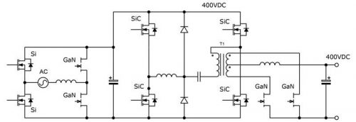
Figure 4: SiC and GaN materials can be successfully implemented throughout a typical power converter.
Takeaways
Silicon carbide (SiC) and gallium nitride (GaN) are two leading-edge semiconductor materials with key benefits including higher voltage operation, wider temperature ranges and increased switching frequencies when compared to existing silicon (Si) technology. The solid benefits that SiC and GaN deliver include significant efficiency gains through miniaturization advancements, decreased cooling requirements and lower overall system costs by as much as 10-20% over traditional Si materials.
Choosing the right partners for your next innovation optimizes efficiency, achieves the best user experience and maximizes profit potential. To get there, Avnet can connect you with our trusted global technology partners including Broadcom, Infineon, Microchip, Nexperia, ON Semiconductor and ST Microelectronics. This enables you to better focus valuable resources on intellectual property innovation and other areas that deliver a strong competitive edge. Together, we provide the support needed to successfully differentiate your product offerings, accelerate your time to market and improve business outcomes.