


JAMES KIM, Senior Semiconductor and Process Integration Engineer | Lam Research
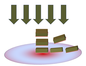
Asymmetries in wafer map defects are usually treated as random production hardware defects. For example, asymmetric wafer defects can be caused by particles inadvertently deposited on a wafer during any number of process steps. In this article, I want to share a different mechanism that can cause wafer defects. Namely, that these defects can be structural defects that are caused by a biased deposition or etch process.


It can be difficult for a process engineer to determine the cause of downstream structural defects located at a specific wafer radius, particularly if these defects are located in varying directions or at different locations on the wafer. As a wafer structure is formed, process behavior at that location may vary from other wafer locations based upon the radial direction and specific wafer location. Slight differences in processes at different wafer locations can be exaggerated by the accumulation of other process steps as you move toward that location. In addition, process performance differences (such as variation in equipment performance) can also cause on-wafer structural variability.
In this study, structural defects will be virtually introduced on a wafer to provide an example of how structural defects can be created by differences in wafer location. We will then use our virtual process model to identify an example of a mechanism that can cause these types of asymmetric wafer map defects.
Methods
deposition on a tilted structure caused by wafer warping
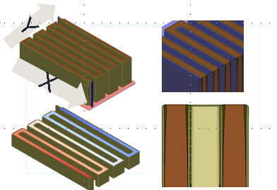
A 3D process model of a specific metal stack (Cu/TaN/Ta) on a warped wafer was created using SEMulator3D virtual fabrication (Figure 1). After the 3D model was generated, electrical analysis of 49 sites on the wafer was completed.
In our model, an anisotropic barrier/liner (TaN/Ta) deposition process was used. Due to wafer tilting, there were TaN/Ta deposition differences seen across the simulated high aspect ratio metal stack. To minimize the number of variables in the model, Cu deposition was assumed to fill in an ideal manner (without voids). Forty-nine (49) corresponding 3D models were created at different locations on the wafer, to reflect differences in tilting due to wafer warping. Next, electrical simulation was completed on these 3D models to monitor metal line resistance at each location. Serpentine metal line patterns were built into the model, to help simulate the projected electrical performance on the warped wafer at different points on the same radius, and across different directions on the wafer (Figure 2).
Using only incoming structure and process behavior, we can develop a behavioral process model and extend our device performance predictions and behavioral trend analysis outside of our proposed process window range. In the case of complicated processes with more than one mechanism or behavior, we can split processes into several steps and develop models for each individual process step. There will be phenomena or behavior in manufacturing that can’t be fully captured by this type of process modeling, but these models provide useful insight during process window development.
Results
Of the 49 3D models, the models on the far edge of the wafer were heavily tilted by wafer warpage. Interestingly, not all of the models at the same wafer radius exhibited the same behavior. This was due to the metal pattern design. With anisotropic deposition into high aspect ratio trenches, deposition in specific directions was blocked at certain locations in the trenches (depending upon trench depth and tilt angle). This affected both the device structure and electrical behavior at different locations on the wafer.
Since the metal lines were extending across the x-axis, there were minimal differences seen when tilting the wafer across the x-axis in our model. X-axis tilting created only a small difference in thickness of the Ta/TaN relative to the Cu. However, when the wafer was tilted in the y-axis using our model, the high aspect ratio wall blocked Ta/TaN deposition due to the deposition angle. This lowered the volume of Ta/TaN deposition relative to Cu, which decreased the metal resistance and placed the resistance outside of our design specification.
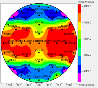
X-axis wafer tilting had little influence on the device structure. The resistance on the far edge of the x-axis did not significantly change and remained in-spec. Y-axis wafer tilting had a more significant influence on the device structure. The resistance on the far edge of the y-axis was outside of our electrical specification (Figure 3).
Conclusion
Even though wafer warpage occurs in a circular manner due to accumulated stress, unexpected structural failures can occur in different radial directions on the wafer due to variations in pattern design and process behavior across the wafer. From this study, we demonstrated that asymmetric structures caused by wafer warping can create top-bottom or left-right wafer performance differences, even though processes have been uniformly applied in a circular distribution across the wafer.
Process simulation can be used to better understand structural failures that can cause performance variability at different wafer locations. A better understanding of these structural failure mechanisms can help engineers improve overall wafer yield by taking corrective action (such as performing line scanning at specific wafer locations) or by adjusting specific process windows to minimize asymmetric wafer defects.