

Researchers at the University of Toronto and the Barcelona Institute of Science and Technology have recently created new solution-processed perovskite photodetectors that exhibit remarkable efficiencies and response times. These photodetectors have a unique design that prevents the formation of defects between their different layers.
“There is growing interest in 3D range imaging for autonomous driving and consumer electronics,” Edward H. Sargent told. “We have worked as a team for years on finding new materials that enable light sensing technologies such as next-generation image sensors and striving to take these in a direction that could have a commercial and societal impact.”


Photodetectors, sensing devices that detect or respond to light, can have numerous highly valuable applications. For instance, they can be integrated in a robotic systems, autonomous vehicles, consumer electronics, environmental sensing technology, fiber optic communication systems ,and security systems.
“In these applications, fast photodetection is required in wavelength ranges beyond human vision,” Amin Morteza Najarian said. “Silicon, the legacy approach—and ideal for electronic readout—does not on its own unite high efficiency with high-speed, as a result of its indirect bandgap, a property of silicon’s band structure that produces weak absorption (hence a need for thick silicon) in the near-infrared.”
In a series of initial computational studies, Sargent and his team identified a binary perovskite with high-carrier mobility and a high absorption coefficient that could compete with currently employed materials in terms of both efficiency and speed. The photodetector introduced in their recent paper is based on this newly identified, active material.
“When light is absorbed by the perovskite active layer, the photogenerated electrons and holes are extracted through electron and hole transport layers,” said coauthor Maral Vafaie. “To achieve fast response times, these charge carriers must move rapidly across the devices, including the transport layers. Nickel oxide (NiOx) is characterized by high crystallinity and mobility, making it an ideal option for hole transport layer (HTL).”
When they first started testing their devices, the researchers found that there was a chemical incompatibility between the established anti-oxidation strategy for PbSn perovskites and the NiOx layer. They thus devised a method to remove oxygen from the device, converting unwanted tin species and ensuring that no harmful residues are left behind.
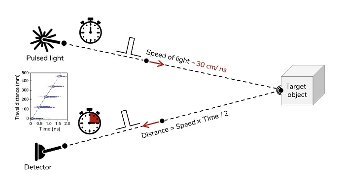
In initial evaluations, the photodetectors created by Sargent, Najarian, Vafaie, and their colleagues achieved very promising results, both in terms of quantum efficiencies and response times. The team also showed that their devices can resolve sub-millimeter distances with a typical 50 µm standard deviation.
“We demonstrated that photodetectors fabricated using binary perovskites convert near infrared light into an electrical signal with an efficiency better than 85% with a response time faster than a fraction of nanosecond,” Sargent and Morteza Najarian said. “This is a 100 times improvement compared to previously reported solution-processed photodetectors. We showcase these performance metrics in spatially resolving sub-millimeter distances, i.e., providing depth resolution.”
In the future, the new solution-processed perovskite photodetectors created by Sargent, Morteza Najarian and their colleagues could prove valuable for creating LiDAR technology (i.e., tools for determining variable distances between objects) and sensors for autonomous vehicles or robots. Meanwhile, the researchers plan to continue searching for advantageous materials and designing new components for sensing technologies.
“In long-range light detection and ranging (LiDAR) applications, only a small fraction of the scattered light from the objects reaches the photodetector,” Sargent and Morteza Najarian added. “If one shifts illumination, and sense, to the short-wave infrared region (e.g., 1550 nm), a higher power of illuminating light becomes possible without posing eye safety issues. We are working on the next-generation III-V semiconductors with this in mind.”