


Panasonic Holdings Corporation announced that it has developed excellent color reproduction technology that suppresses color crosstalk by thinning the photoelectric conversion layer using the high light absorption rate of the Organic Photoconductive File (OPF) and by using electrical pixel separation technology. In this technology, the OPF part that performs photoelectric conversion and the circuit part that stores and readouts the electric charge are completely independent. This unique layered structure dramatically reduces the sensitivity of each pixel in green, red, and blue in wavelength regions outside the target range. As a result, color crosstalk is reduced, excellent spectral characteristics are obtained, and accurate color reproduction is made possible regardless of the type of light source.
Abstract
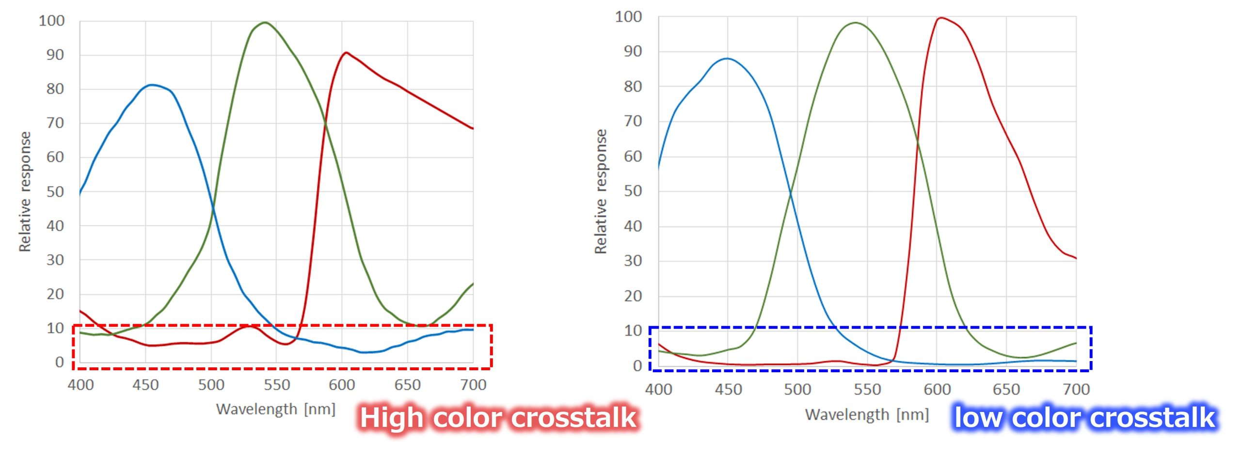
Conventional Bayer array-type silicon image sensors do not have sufficient color separation performance for green, red, and blue. Therefore, for example, under light sources that have peaks at specific wavelengths, such as cyan light and magenta light, it has been difficult to accurately reproduce, recognize, and judge colors.


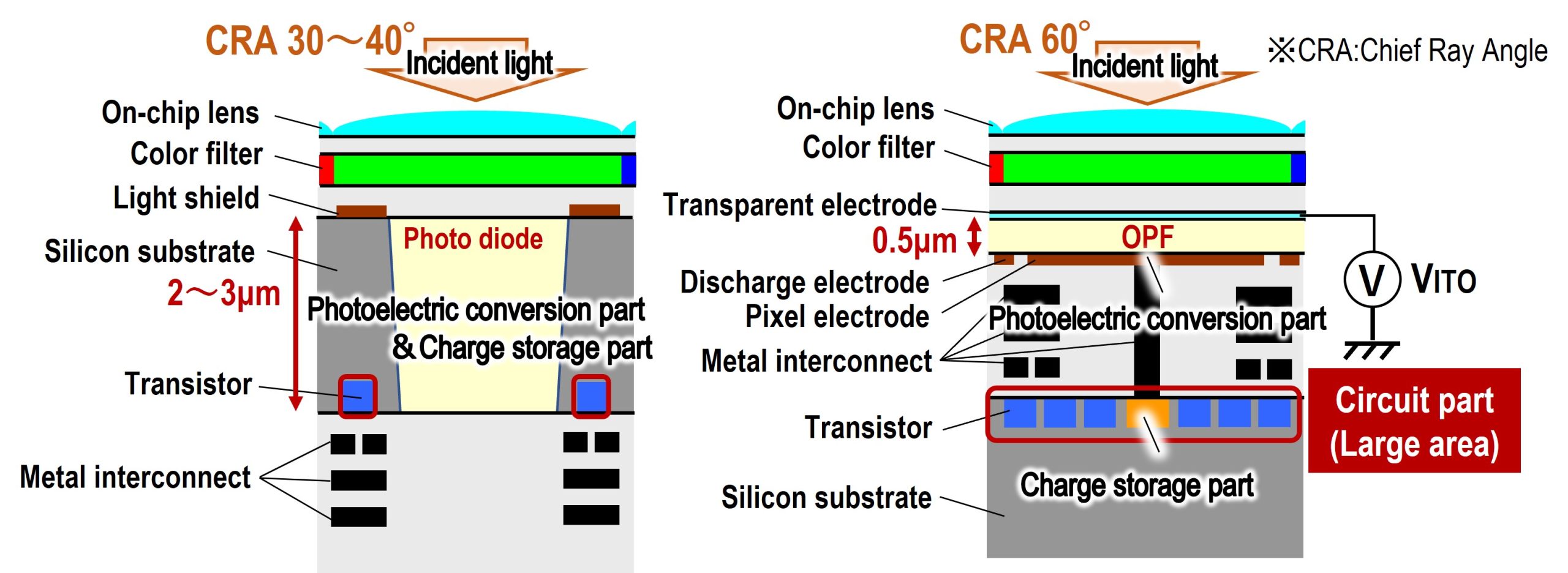
Our OPF CMOS image sensor has a unique structure in which the photoelectric conversion part that converts light into an electric signal is an organic thin film, and the function of storing and reading out the signal charge is performed in the circuit part, which are completely independent from each other (Figure 1). As a result, unlike with conventional silicon image sensors, it is possible to provide photoelectric conversion characteristics that do not depend on the physical properties of silicon. The OPF with its high light absorption rate enables the thinning of the photoelectric conversion part ((1) Photoelectric conversion film thinning technology). By providing a discharge electrode at the pixel boundaries, the signal charge due to the incident light at the pixel boundaries is discharged, and the signal charge from adjacent pixels is suppressed ((2) Electrical pixel isolation technology). In addition, since the under part of the OPF is covered with the pixel electrode for collecting the signal charge generated in the OPF and the electrode for discharging the charge, incident light that cannot be absorbed by the OPF does not reach the circuit side. This suppresses the transmission ((3) Light transmission suppression structure). With the above three technologies, it is possible to suppress light and signal charges that enter from adjacent pixels. As a result, color crosstalk can be reduced to an almost ideal shape, as shown in the spectral characteristics shown in Figure 2, and accurate color reproduction is achieved regardless of the color of the light source (Figure 3).
This technology enables accurate color reproduction and inspection even in environments where it is difficult for conventional image sensors to reproduce the original colors, such as plant factories that use magenta light. It is also possible to accurately reproduce the colors of substances with subtle color changes, such as living organisms. It can also be applied to managing skin conditions, monitoring health conditions, and inspecting fruits and vegetables. Furthermore, in combination with the high saturation characteristics and global shutter function of our OPF CMOS image sensor*, it can contribute to highly robust imaging systems that are highly tolerant of changes in light source type, illuminance, and speed.
BSI Si CMOS image sensor / OPF CMOS image sensor
Figure 1. Comparison of pixel structure (cross-sectional image)
BSI Si CMOS image sensor / OPF CMOS image sensor
Figure 2. Comparison of spectral characteristics
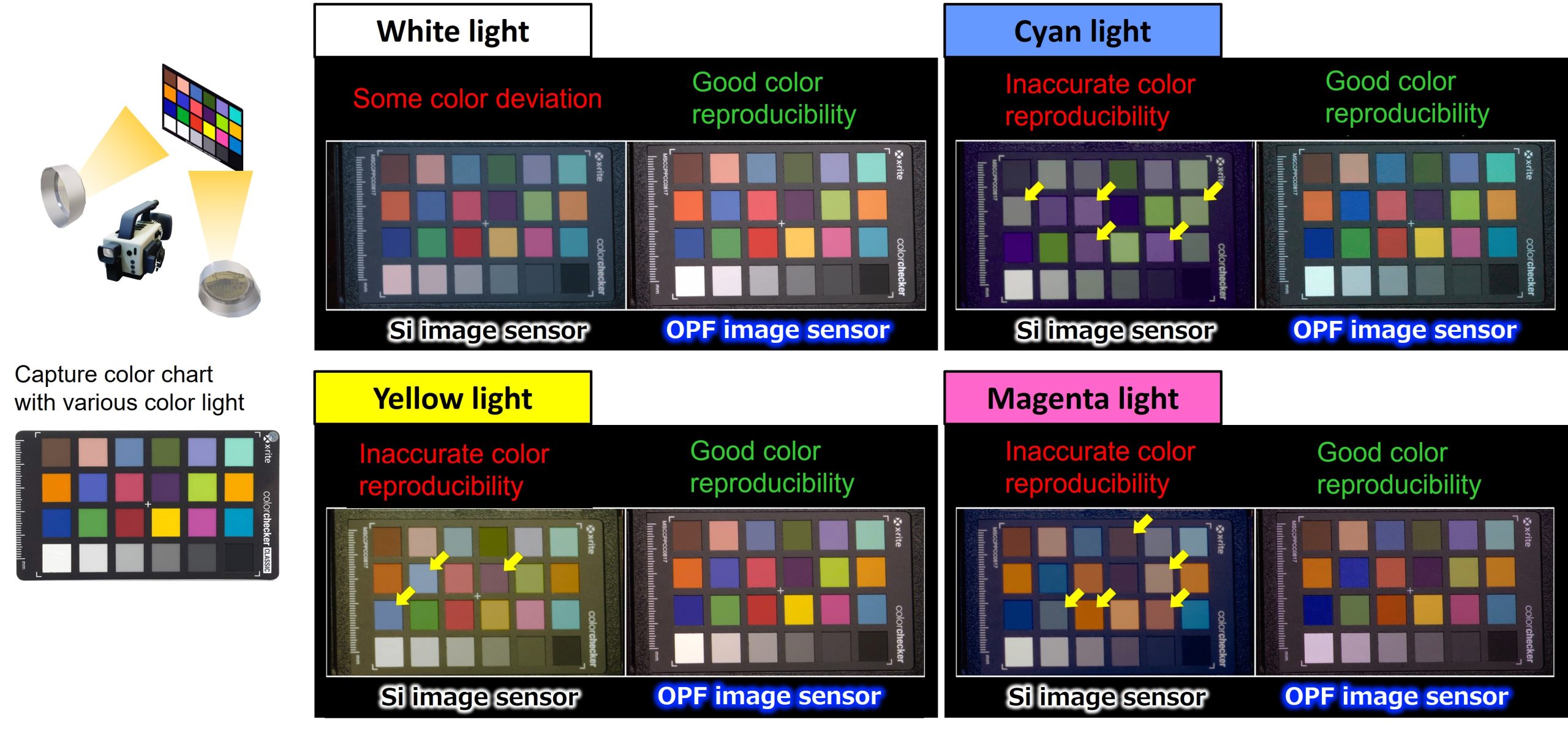
Figure 3. Comparison of color chart imaging under various light sources
Main features
This development is based on the following technologies.
- Photoelectric conversion film thinning technology with 10 times higher light absorption
- Electrical pixel isolation technology that discharges unnecessary charges at pixel boundaries
- Light transmission suppression structure that suppresses the transmission of light through the photoelectric conversion part
Details of the technologies
1. Photoelectric conversion film thinning technology with 10 times higher light absorption
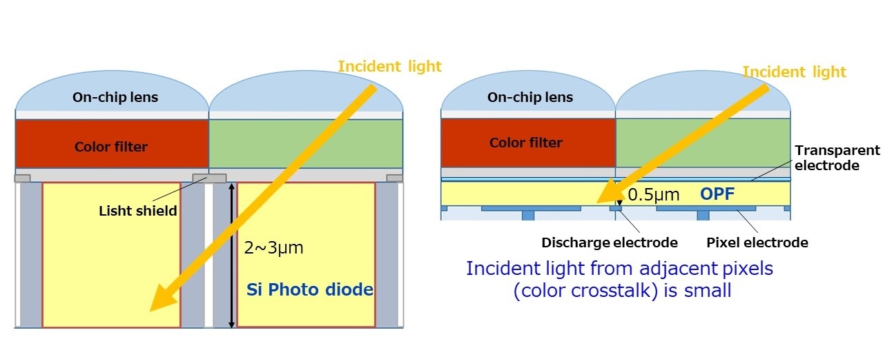
The light absorption coefficient of the OPF that was developed this time is about 10 times higher than that of silicon (Figure 4). The distance required for light absorption is shortened, allowing for the OPF to be designed thinner than silicon photodiodes, and in principle, it is possible to reduce oblique incident light from adjacent pixels, which is a factor in color crosstalk (Figure 5).
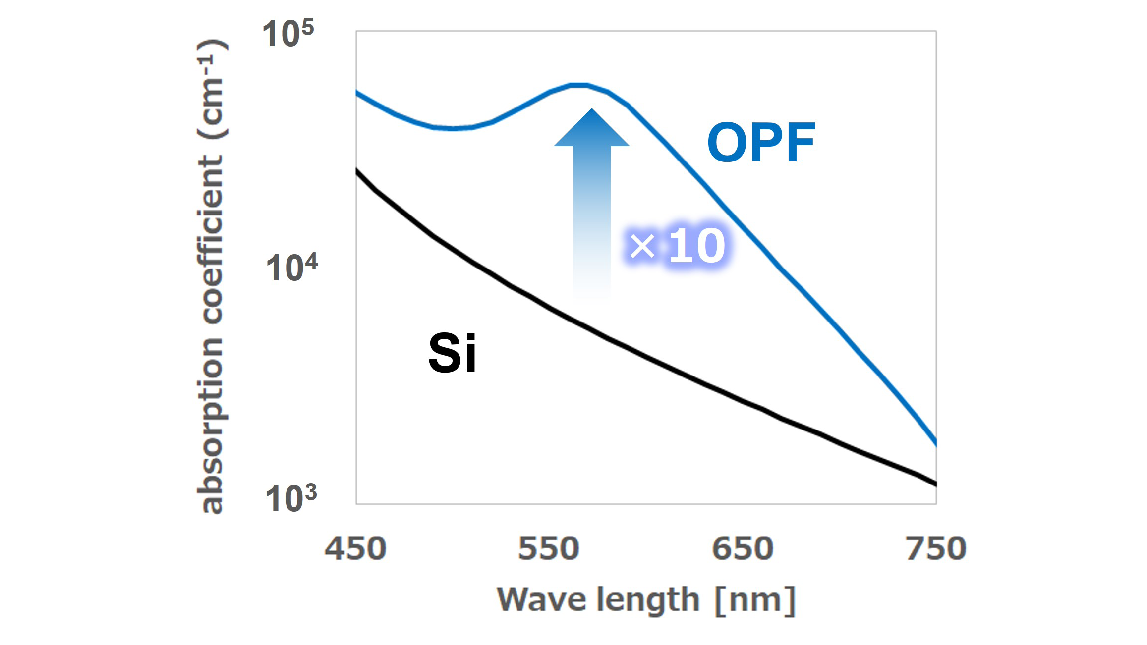
Figure 4. Optical absorption coefficients of OPF and Si
BSI Si CMOS image sensor / OPF CMOS image sensor
Figure 5. Comparison of the effects of oblique incident light
2. Electrical pixel isolation technology that discharges unnecessary charges at pixel boundaries
The charges generated at the pixel boundaries include signal charges originating from adjacent pixels due to oblique incident light, which contributes to color crosstalk and resolution degradation. In conventional silicon image sensors, a light-shielding layer is provided at the boundary between pixels to prevent oblique incident light. However, the light reflected by the light-shielding layer becomes stray light and penetrates into adjacent pixels, and is diffracted to wrap around, resulting in insufficient light-shielding.
Therefore, Panasonic has developed a structure that discharges the signal charge caused by the incident light at the pixel boundaries and suppresses the intrusion of signal charge from the adjacent pixels by placing a new discharge electrode at the pixel boundaries. As shown in Figure 6, by providing a discharge electrode, the charge generated at the pixel boundaries is discharged, allowing for image quality deterioration to be suppressed.
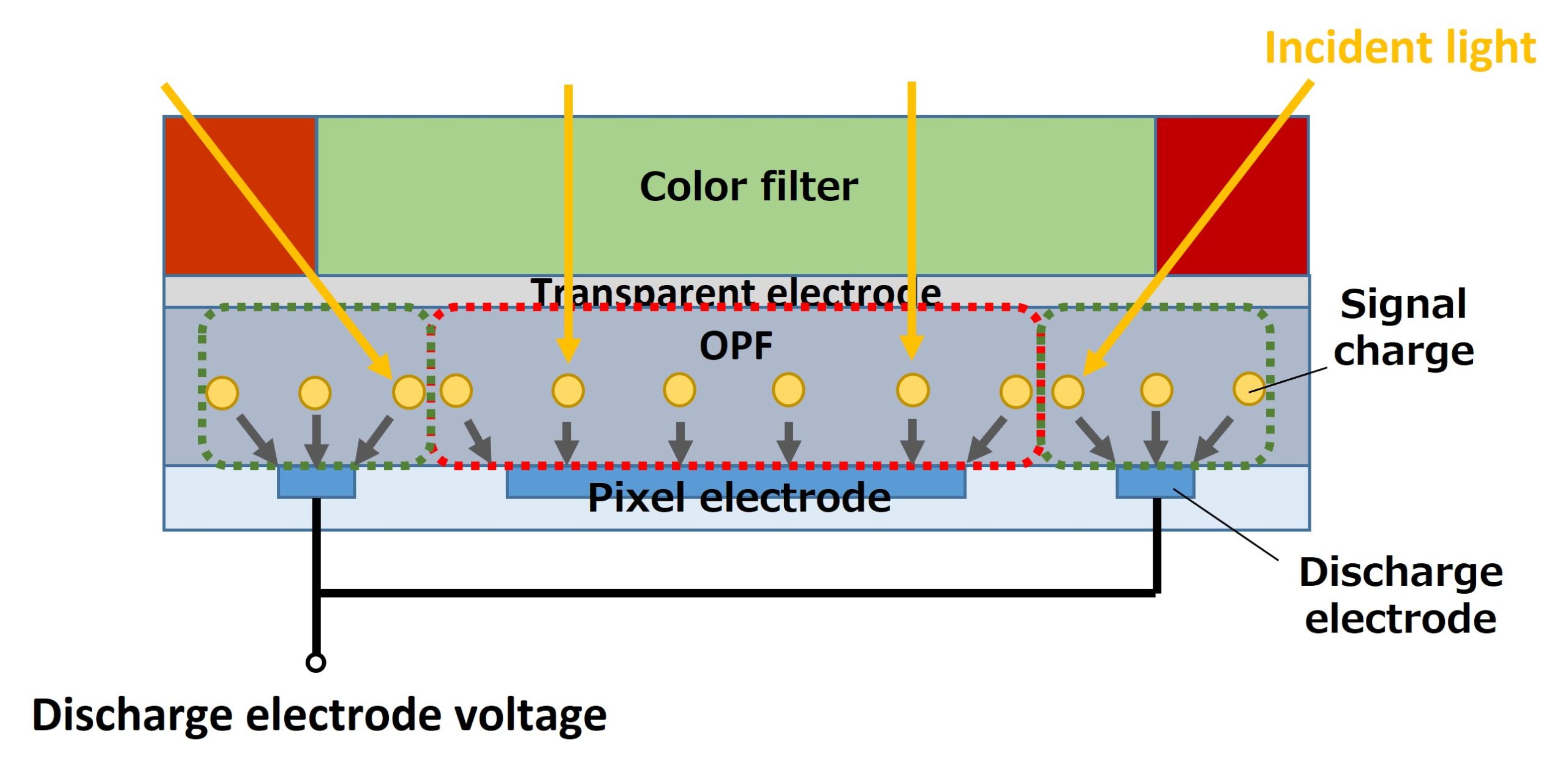
Figure 6. Signal charge in OPF
3. Light transmission suppression structure that suppresses the transmission of light through the photoelectric conversion part
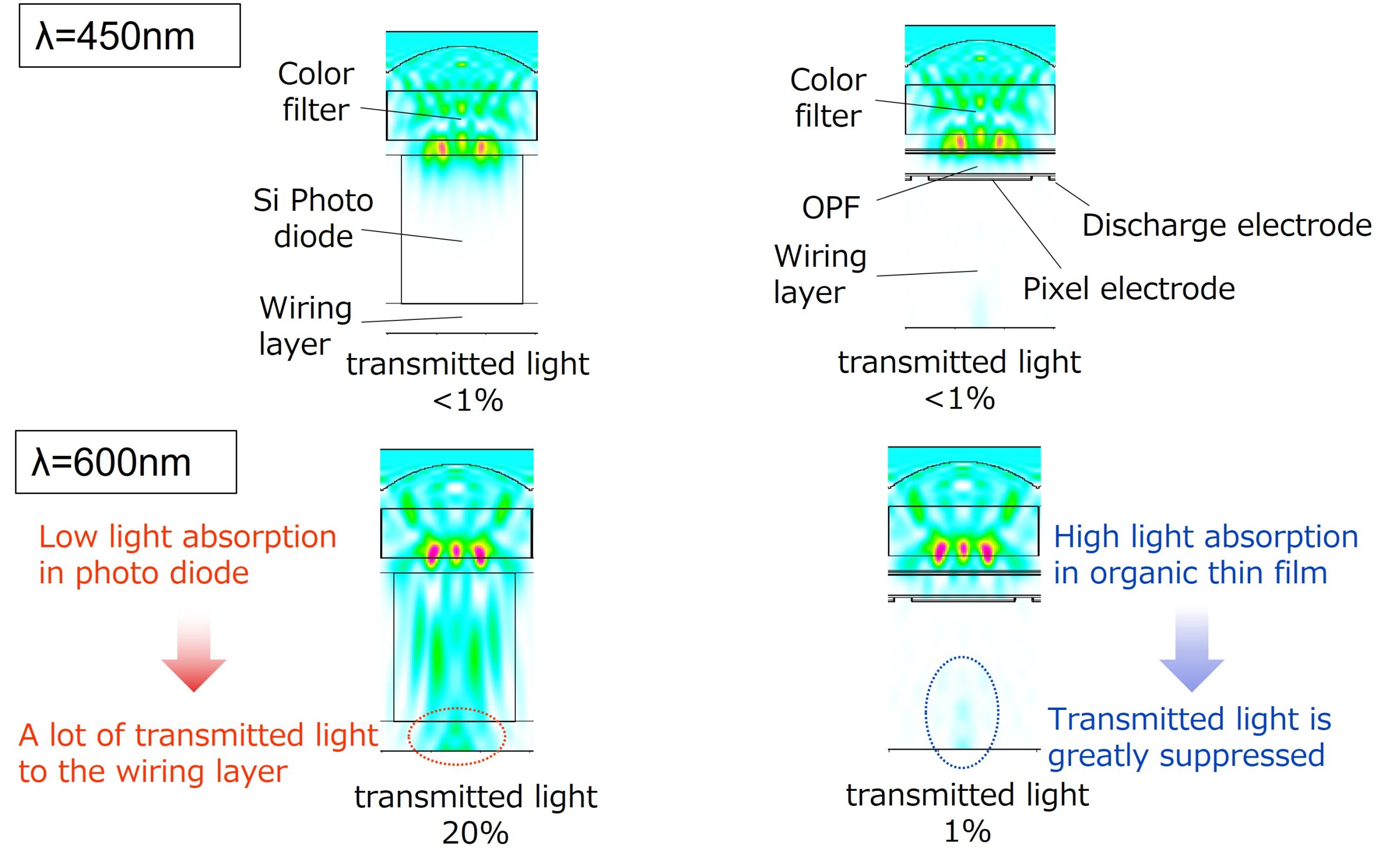
Light incident on the photoelectric converter (photodiode in silicon image sensors, OPF in OPF CMOS image sensors) is photoelectrically converted into signal charges. However, part of the light is not photoelectrically converted and passes through, contributing to color crosstalk. Red light, which has a longer wavelength and lower energy compared to another light, is easier to penetrate and has greater crosstalk. As shown in Figure 7, a silicon image sensor transmits approximately 20% of light with a wavelength of 600 nm, while an OPF CMOS image sensor transmits only 1% of light with the same wavelength. The bottom of the OPF is covered with a pixel electrode for collecting signal charges and an electrode for discharging charges. Therefore, incident light that cannot be completely absorbed by the OPF is absorbed or reflected by the electrode, and the reflected light is again absorbed by the OPF. Furthermore, since the space between the pixel electrode and the discharge electrode is very small, it is difficult for light to pass through the lower part of the OPF. As a result, OPF CMOS image sensors are structurally very tolerant of color crosstalk.
BSI Si CMOS image sensor / OPF CMOS image sensor
Figure 7. Light intensity simulation at pixel cross section
In the future, we will propose these OPF CMOS image sensor technologies for various applications such as commercial broadcasting cameras, surveillance cameras, industrial inspection cameras, and automotive cameras. We will also contribute to highly robust imaging systems that are highly tolerant of changes in light source type, illuminance, and speed (Figure 8).
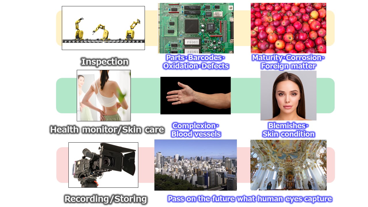
Figure 8. Application example of OPF CMOS image sensor