


Abstract
Adding USB-C ports to optimize mobile computing systems is gaining increasingly more attention these days. Charging the mobile computing battery through USB-C has become a new trend. To further explain the increase in using USB-C ports, this document will first review the conventional USB-C NVDC buck-boost charger topology and outline its pros and cons. It will then discuss a combo battery charger solution from Renesas, which is able to operate in NVDC and the new Hybrid Power Buck-Boost (HPBB) mode as well.


Introduction
The USB-C interface is revolutionizing the way we charge our electronics devices, particularly in mobile computing devices. Conventional mobile computing devices, such as laptop or notebook computers, include a dedicated and typically proprietary plug-in port for a power adapter. The battery charger will be responsible for charging the battery when the adapter is plugged in to this dedicated port, in addition to controlling the supply of power to the system.
Recently, some mobile computing device manufacturers have moved towards adding USB ports, supporting the newer USB Type-C (USB-C) or USB Power Delivery (USB PD) protocols. USB-C supports bi-directional power flow at a much higher level than previous versions of the USB interface; e.g., 5 V. Starting from a default 5 V voltage, the USB-C port controller can negotiate with the plugged-in device to raise the port voltage to 12 V, 20 V, or another mutually agreed upon voltage, at a mutually agreed upon current level. The maximum power a USB-C port can deliver is 20 V at 5 A current, which is 100 W of power and more than adequate to charge a computer. As a result, charging mobile computing devices through the USB-C port is becoming more popular as compared to conventional charging through the typical separate and proprietary power adapter port.
USB-C Buck-Boost NVDC Charger Topology
This new USB-C protocol provides a wider range of variable input voltages (Vin) to a battery charging system, which could be lower or higher than battery pack voltage and system bus voltage. Hence, the buck-boost converter becomes the most favorable option. Figure 1 shows the simplified diagram for a conventional narrow voltage DC (NVDC) four-switch buck-boost charging topology. This NVDC charger is comprised of four switching FETs belonging to the buck-boost converter and one BFET between the battery and system voltage bus, Vsys. The input of the buckboost converter could be from a proprietary AC/DC wall adapter or from the USB-C port.
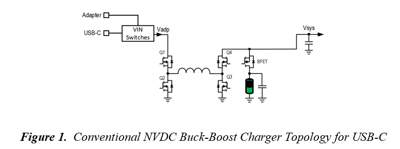
Figure 2 shows the power path when input power is present. There are three operation scenarios in this mode.
- If the battery is fully charged, the buck-boost charger will turn off the BFET. In this case, the buck-boost charger provides the output power to the system with Vsys regulated to the desired voltage.
- If the battery is not full and the buck-boost charger is charging the battery, the BFET is turned on. In trickle charge mode, the BFET operates in the saturation region to behave like a linear regulator (LDO), and Vsys is regulated at the target voltage. If the charger is in CC or CV mode with the BFET fully turned on, Vsys is equal to Vbat (assume no voltage drop from the BFET). Input power = system power + battery charge power, with the assumption of input power > system power.
- It doesn’t matter if the battery is in charge status or not. As soon as the system power > input power, Vsys will show a dip. In general, the body diode in the BFET will conduct if the Vsys< Vbat-Vdrop, where the Vdrop stands for the body diode drop with a typical voltage of 0.7 V. Otherwise, with a more sophisticated control, the BFET could be turned on earlier to ‘catch up’ and support Vsys. In either case, the battery will be discharged and the battery power merged with the input power to support the system power.
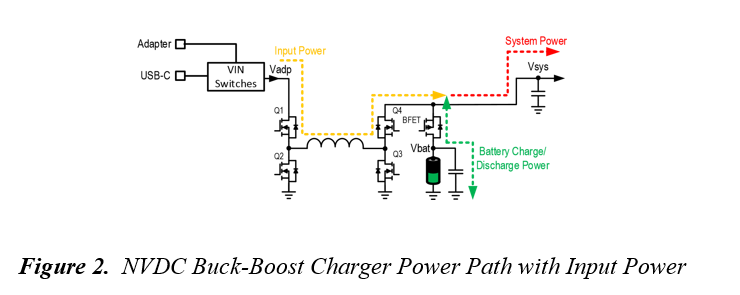
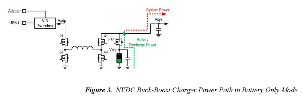
Figure 3 shows the power path in battery-only mode. This mode is relatively simpler than the previous one because the battery always provides power to the system with the BFET forced on. Vsys is equal to Vbat in this mode.
 One of the typical features of a NVDC configuration is that all power flows through and is processed by the buckboost charger, making power loss inevitable due to MOSFET switching and conduction loss, inductor core loss, copper loss, etc. The power inductor needs to be sized correctly to handle the full system’s power, plus the charging power, therefore demanding a bigger inductor. Thus, a NVDC configuration is preferred for a lower power level system; e.g., 60 W or lower. One advantage of a NVDC configuration is a simple control scheme. When the system enters turbo mode, where system power is higher than adapter power, it’s not necessary that the charger controls anything beyond the adapter current control. The battery naturally discharges the current through the BFET to automatically support the system.
Renesas New Hybrid Power Buck-Boost (HPBB) Configuration
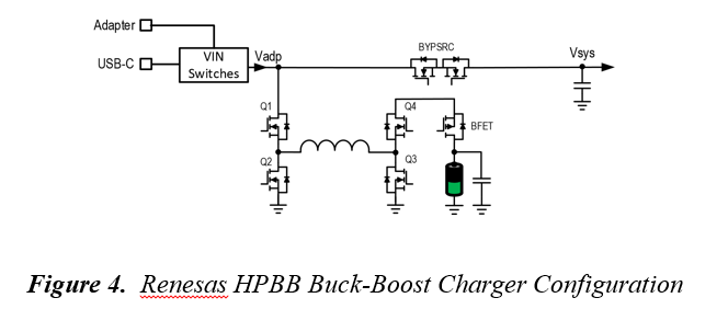
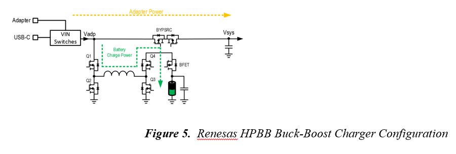
Figure 4 shows the new HPBB battery charger configuration. In this mode, the input power passes through bypass
FETs instead of going through the buck-boost charger. Thus, the power loss is greatly reduced compared with the NVDC mode. The buck-boost charger only processes the battery charge/discharge power, and a larger inductor is not required for this configuration.
 When input power is present, there are two operation scenarios for this mode:
- Input power > system power: If this condition is met, the buck-boost battery charger will not provide power to the system. Instead, the buck-boost charger can be in standby mode if the battery pack is fully charged or it is charging the battery pack. Figure 5 shows the power path in HPBB mode for this scenario.
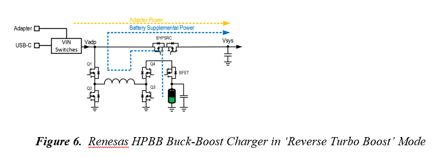
 2. Input power < system power: In this case, the battery needs to be discharged, and the buck-boost charge is operating in reverse mode to pump energy from the battery to the Vadp side. The battery power combines with the input power to support the system’s power. This mode is also called ‘Reverse Turbo-Boost’ mode, and Figure 6 shows its power path in HPBB mode.
 Introducing the Renesas ISL9241 ‘Combo’ Buck-Boost Battery Charger
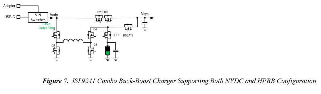
The ISL9241 is the latest buck-boost charger product from Renesas. It is the industry’s only USB-C buck-boost charger supporting both NVDC and HPBB configurations.
In NVDC mode, the ISL9241 automatically selects the adapter and/or the battery as the source for system power. ISL9241 NVDC operation also supports turbo mode by turning on the BGATE FET to limit the adapter current at the adapter current limit set point while the battery supplies the rest of the power required by the system.
In HPBB mode, the ISL9241 supports bypass, bypass + charging, reverse turbo-boost mode, etc.
By allowing both HPBB and NVDC configurations, the ISL9241 brings extra flexibility to customers’ designs and offers optimized system performance. These two modes are reconfigurable by host firmware in the EC (embedded system controller) when different power sources are used such as an AC/DC adapter or inputs from USB-PD ports.
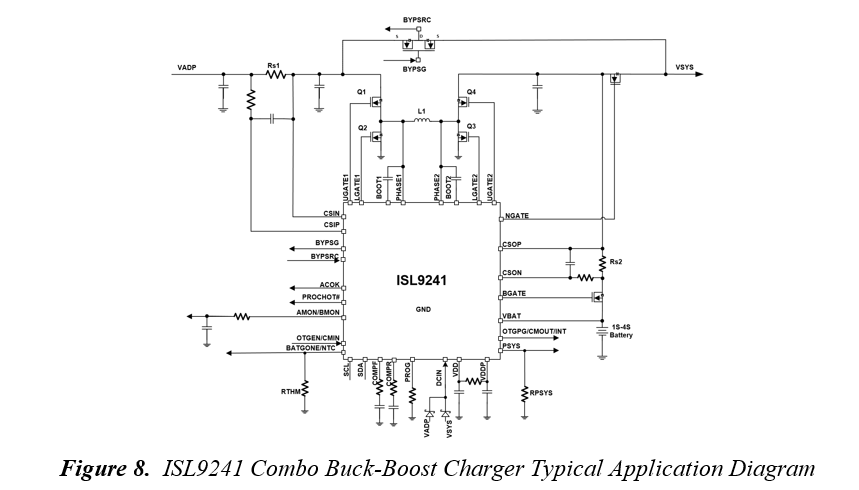
 The ISL9241 provides the charging function, system bus regulation, and protection features using only NFETs for efficiency and BOM cost optimization. The advanced Renesas R3 Technology is used to provide a highly efficient light-load charging mode. ISL9241 reconfigurability of the compensation allows a smaller inductor and higher efficiencies optimized for multiple power levels.
The ISL9241 takes input power from a wide range of DC power sources (conventional adapters, travel adapters, USB type-C power ports, etc.) and safely charges battery packs with up to four-cell Li-ion series batteries. The ISL9241 also provides autonomous charge with automatic EOC (end of charging). The bypass mode for HPBB uses the controller’s firmware, allowing the adapter to provide power to the system directly.
The ISL9241 supports reverse buck, boost, or buck-boost operation to the adapter port (OTG mode) from battery packs with two- to four-cell batteries. This will allow configurations to support USB-C Power Delivery (PD) output for Programmable Power Supply (PPS) ports. The ISL9241 can operate with only a battery, only an adapter, or both connected. The system power can be provided from the adapter, battery, or a combination of both. For Intel IMVPcompliant systems, the ISL9241 includes System Power (PSYS) monitor functionality, which provides an analog signal representing total platform power. The PSYS output will connect to a wide range of IMVP core regulators to provide an IMVP-compliant power domain function. The ISL9241 also has a processor-hot (PROCHOT#) monitor and supports Supplemental Mode, which meets Intel’s Vmin Adaptive Protection (VAP) requirement by keeping the battery voltage above a defined minimum voltage level. ISL9241 serial communication uses SMBus/I²C, which allows programming of many key parameters to deliver a customized solution.
The ISL9241 keeps monitoring its operation and communicates its fault/warning status through interrupt. The integrated 8-bit ADC in the ISL9241 enables key system parameter telemetry, such as temperature (PCB and junction), adapter current/voltage, battery charge/discharge current, and system bus voltage.
The ISL9241’s reconfigurable charging architecture allows users to flexibly utilize the charger for multiport configurations to meet the system’s design requirements. Its multi-port USB-C support enables user to create a multiport USB-C system and still be 100% compliant to the USB-PD 3.0 standard.
The ISL9241 has an input voltage range of 3.9 V to 23.4 V, with an output of 3.9 V to 18.304 V for two- to four-cell battery packs; up to 20 V On-The-Go; and can also be enabled for autonomous charging and end of charge without communication from an embedded controller. Automatic sensing allows the device to enter trickle charging mode when the battery is depleted; it has an available setting for a two-level adapter current limit; and the battery learn mode calibrates the battery fuel gauge. Programmable features using the SMBus or I2C interface provide the user with flexibility in their design.
Design Tools from Renesas
Evaluation Board/User Guide
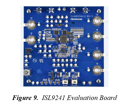
An evaluation board and detailed user guide for customer testing and evaluation are available for the ISL9241. A photograph of the evaluation board is shown in Figure 9.
 ISL9241 GUI
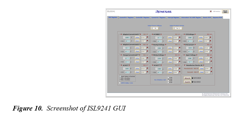
The ISL9241 GUI software offered by Renesas will help accelerate the design, testing, finalization, and debugging of your battery charger design. It connects to development boards to set various adjustable system parameters and threshold values. Figure 10 shows an example of ISL9241 GUI software windows.
 Conclusion
This white paper gives an overview of today’s battery charging topologies and operating principles for consumer mobile computing devices like notebooks. The battery charger is the critical component for mobile device power management because it not only charges the battery packs, but also manages the entire power flow from adapter to computing device. The battery charger in the computing system is required to work seamlessly with other system management devices, such as the embedded controller (EC), to support system power demands efficiently. The ISL9241 offers increased flexibility by providing both NVDC and HPBB configurations, which allow selection between these two modes to optimize the battery charger design. The ISL9241’s register map is highly compatible with Renesas’ other existing charger products such as the ISL9238. Thus, it greatly reduces the development effort when migrating the battery charger design with other Renesas charger products when designing with the ISL9241. In addition, the firmware in the EC for the NVDC mode only requires a minor revision to enable the ISL9241 to operate in the HPBB mode, which reduces development and qualification efforts when using the ISL9241 across multiple computing platforms.
Article Courtesy: Renesas Electronics