Temperature control is one of the key factors for a MOSFET or IGBT power module to work efficiently. Although some MOSFETs are equipped with an internal temperature sensor (body diode), there are other ways to monitor and control temperature. A semiconductor silicon PTC resistor can be used with well-defined current control or a Pt- or Ni-based resistance temperature detector (RTD) with moderately low resistance values and more linear performance. Whether the sensor is an SMD, a wire bonded die, or even a sintered die, an NTC thermistor remains the most sensitive and versatile temperature sensor. When designed properly, it will ensure the proper derating and eventual shutdown of the module in case of overheating or excessive external temperature.
In this article we will focus on a bondable NTC die and adopt the path of analog electronic simulation to show how fundamentally a derating and a shutdown can be operated in a power module. Why analog? It’s the best way to simplify things and illustrate the different phenomena in a visual way. It’s also ideal for developing an intuitive application. The last motivation is pecuniary: we will develop a simulation within the limits of a free software (LTspice), while other design tools would possibly allow for more sophisticated designs.


So, let’s take the LTspice design in Figure 1, which is a simple boost converter design. However, thanks to the versatility of LTspice, the IGBT and the diode models have been replaced with thermal models, where the heat fluxes are explicitly represented with an output pin, allowing them to be connected to a thermal circuit (the heatsink, for example). We will here use a simple RC circuit (in the real world, the designer would need to carefully define the Zth model as a Cauer or a Foster model).
Figure 1
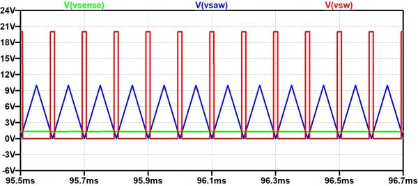
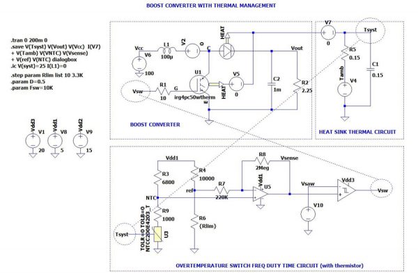 During the converter’s operation, the heat flux results in a hot spot (the voltage at the node Tsyst in this case, which is the temperature to control). This temperature is input into an NTC model (Vishay wire bondable die NTCC200E4203_T). The NTC signal is used via a Wheatstone bridge, compared to a threshold, amplified, and compared to a sawtooth signal (Vsaw). The final output Vsw is the pulse signal applied at the gate of the IGBT. Under the temperature threshold defined by the Rlim resistor value, we apply a 100 % full duty cycle pulse at the IGBT’s gate. When there is overheating — produced by the IGBT and the diode — cumulated with the ambient temperature (the voltage at the node Tamb in the thermal circuit), the duty cycle is reduced and the output / input ratio of the buck converter (Vout / Vcc) will be reduced. This produces less heat and the temperature begins to stabilize. At the limit above a certain temperature, this ratio must be reduced to 1.
In order to perform a simulation within a reasonable time, we must scale down the thermal capacity of the heatsink. Thermal increases can take minutes or even hours, and we want to visualize them within a very short time.
Here are the results of the simulation: in each figure, the results are shown with or without temperature derating (in order to eliminate the temperature control, the Rlim value is taken as very low).
Figure 2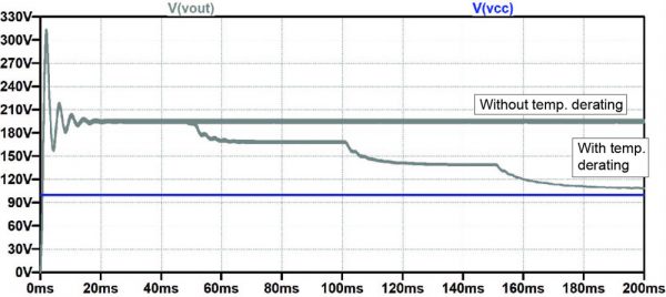
Figure 3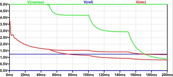
Figure 4
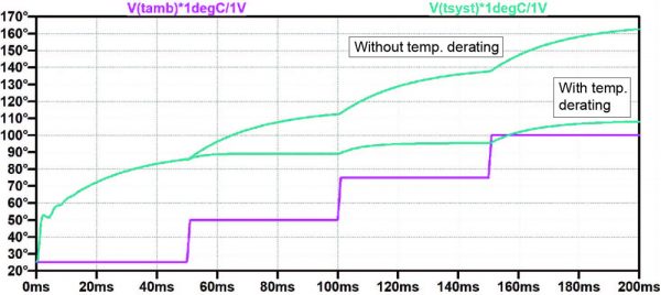 In Figure 2, you will notice the usual oscillating, non-optimized behavior of a boost converter during the first 20 ms. The temperature Tsyst (Figure 4) begins to increase, and then when the ambient temperature increases, the derating Vout / Vcc begins when the Tsyst reaches 90 °C. Every further increase of the ambient temperature decreases the duty cycle until the total deactivation of the boost converter. At 110 °C, the derating is maximum.
Without temperature protection, Tsyst can reach 160 °C to 170 °C (Figure 4). In real power modules, peak die temperatures could reach 200 °C or more.
The voltages Vsense, Vntc, and Vlim are shown in Figure 3. The variation of the duty cycle is also illustrated at different times in Figures 5 and 6.
Of course, all the thresholds are scalable and the switch threshold can be adapted accordingly.
Figure 5
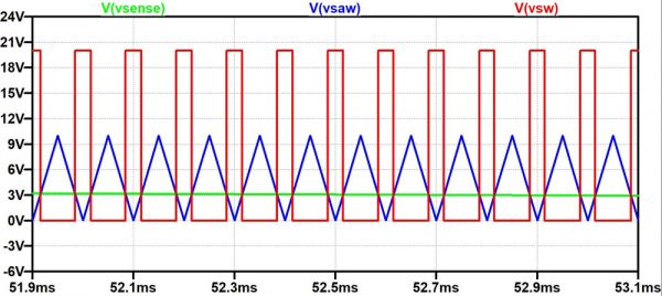
Figure 6
 Going further into more complex simulations, we can also try to reproduce a full-bridge IGBT module (as shown in Figure 7). This circuit produces a 50 Hz sinusoidal current through an inductive load, with an IGBT switching at 30 kHz. The gate driver stimulation circuit will deliver a constant frequency up to 125 °C and will reduce the duty cycle in order to mitigate the IGBT losses above this temperature.
Figure 7
 In Figure 8, we visualize the sum of the heat-power produced by the IGBT’s switching (I(V6) expressed in W), together with temperature (V(Tsyst) expressed in degrees Celsius) increase in time. The produced current is also shown in the lower pane of Figure 8.
Figure 8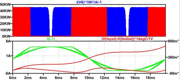 Without entering into the details, it is possible to mitigate the temperature increase (Figure 8 lower pane, red curves) in time by playing into the modulation parameters: a reduction of switching duty time will reduce the heat production, but will also result in a less sinusoidal signal.
We will not go further in the details of this case, but we hope to have shown with the provided examples that LTspice circuit simulations with NTC thermistors can be pushed very far and can help a MOSFET / IGBT power module design engineer to develop their intuition about their circuit, and help them to mitigate the crucial thermal aspects related to circuit protection.
The simulations shown in this article are available on request at edesign.ntc@vishay.com and can be downloaded at:
https://www.hackster.io/alainstas/spice-simulation-of-temperature-derating-of-boost-converter-5acef8
https://www.hackster.io/alainstas/ltspice-inverter-simulation-with-thermal-effects-dadf6a