

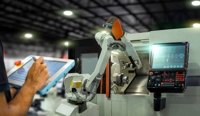
MOSFET improves switching frequency and conversion efficiency
Since the introduction of SMPS into the market in the 1970s, the traditional non-isolated buck regulator architecture has remained essentially unchanged, consisting of two switches or one switch and one diode. The two switches operate out of phase with one another, a “high side” series switch that conducts current to a load limited by a series inductor with stored energy, and a “low side” switch that allows current to continue to flow into the load while releasing energy from the inductor.


By the mid-1980s, silicon metal oxide semiconductor field effect transistors (MOSFET) were introduced, allowing switching frequencies to increase from 20-30 kHz to 200-300 kHz. This increased the frequency leads to a proportionate reduction in the size of the inductor. The use of FETs also increases conversion efficiency by about 10% (from typically 60-70% to 70-80%) and helps accelerate switching transitions, thereby improving EMI performance.
According to Moore’s Law, power conversion is still an analog function and cannot be scaled in silicon. Therefore, the size of silicon remains essentially unchanged. As the material improves, the filtering capacitance technology changes considerably and the capacitor structure decreases. In addition, buck regulators now use multilayer ceramic capacitors (MLCCs) as input and output filters and conductive polymer tantalum solid capacitors (POSCAPs) for bulk capacitance as required. Changes in the inductor are very little and remain wound components for as long as a few amperes or more, typically accounting for 50 percent of the total board space for power conversion. As a result, the inductor has become a problem component that determines the size and height of the overall solution. Any attempt to reduce the size of the solution by reducing inductance implies an increase in switching frequency, a corresponding decrease in efficiency, and an increase in EMI.
New power architecture pursues smaller size and higher efficiency
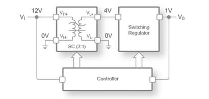
In pursuit of smaller sizes and higher efficiency power conversion, Murata brings a new power architecture to the market that allows switching frequencies to remain in the range of 1-2 MHz while reducing the required inductance and improving overall power conversion efficiency. Murata uses a patented two-stage architecture, including a charge pump with SMPS (also known as a switched-capacitor converter). Charge pumps are highly proprietary technologies that solve some of the fundamental problems traditionally associated with the poor efficiency and high EMI of charge pumps.
Murata’s two-stage architecture is not a single-stage buck. All work is performed by two switches and one inductor. Input and output voltages are slewed across the inductor. The whole voltage is converted into many small voltage steps in both the input and output steps. In addition, the current using the two-stage architecture flows almost continuously into the system compared to the substantial current pulses seen in the traditional single-stage buck circuits.
The net result of this two-stage architecture is that Murata’s conducted and radiated EMI architecture produces much lower EMI signature because the major source of EMI in single-stage bucks circuits is inductors, since Murata uses much less inductance in the system and therefore naturally eliminates most EMI sources.
This two-stage buck architecture is an architectural innovation using standard “off-the-shelf” FETs in very mature CMOS semiconductor processes. Since the inductor is no longer a dominant component in the bill of materials, the power conversion is reduced from 30-40% of the usual system circuit area to half without compromising efficiency. Finally, since the inductor is normally one of the tallest components in the system, this architecture can provide a thinner solution, increase packing density, and make mobile products slimmer.
Power semiconductors providing lossless voltage reduction conversion
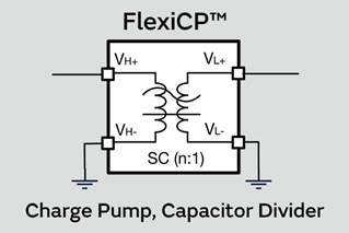
The PE252xx series of the FlexiCP™ power semiconductor introduced by Murata is based on Murata’s proprietary ultra-high efficiency capacitor divider product from its adiabatic or lossless charge pump technology. This technology is well suited to provide a “lossless” step-down voltage conversion for the intermediate bus system to support the downstream point-of-load and achieve the highest level of efficiency, an IC based on an integrated charge pump control architecture integrated with an FET that can be connected in parallel to scale to high power system requirements.
Murata charge pumps can imagine it as a virtually lossless DC transformer with a very small volume that supports open-loop Vout tracks Vin, where Vout is a fixed ratio of Vin (i.e., ÷2, ÷3, ÷4 or ×2, ×3, ×4, etc), may have several ratios within one part (e.g., ÷2, ÷3), and the efficiency remains approximately the same irrespective of the ratio (≈97%), has low-ripple, EMI, noise phase interleaved and soft switching, and can inherently be handled in parallel.
PE25200 in the FlexiCP™ Power Semiconductor Series is a user-selectable divide-by-2 or 3 charger pump capacitor divider IC with an integrated FET that provides up to 45 watts of power at a peak efficiency of 97% and a divider ratio between 2 and 3 enables to converts 2- or 3-cell lithium platforms to 1-cell platforms in mobile computing applications.
PE25200 devices can also use front-end DC-DC converters as part of the 12Vin point-of-load design, and can be applied to FPGA, DDR memory, and ASICs that power datacenter, networking, and optical equipment. PE25200 devices are WLCSP packaged, enable, power good, frequency synchronization, cycle Skipping, have over current protection, over-temperature protection, UVLO, parallel operation, etc.
Typical applications of PE25200 include two-cell and three-cell lithium platforms, ultrabook and notebook, full-size tablets, and products designed with ultra-thin form factor designs, as well as 12VIN point of load designs in networking and telecommunications. Murata also launched the PE25200 Evaluation Kit (EVK) to allow customers to test DC-DC converters.
Another Murata power semiconductor, the FlexiCP™ PE25204, is an ultra-high efficiency front-end DC-DC converter solution that divides the input voltage into three or four voltages and provides up to 72 watts of power at a peak efficiency of 97% for the capacitor divider IC of the 48V divide-by-4 charge pump capacitor with an integrated FET.
PE25204 devices can be connected in parallel to increase output power. The input voltage ranges from 18V to 60V and is supported in divide-by-4 operation, and ranges from 18V to 45V in divide-by-3 operation. PE25204 provides products suitable for data centers, network routers, base stations and optical equipment, and is a high-power, high-efficiency solution for 48V to 12V step-down conversion applications.
PE25204 is WLCSP packaged and can use capacitors in a very thin 1 mm high solution. It supports enable, power good, frequency synchronization, over current protection, over-temperature protection, UVLO, parallel operation, and can be used in ultrabooks/notebook, data centers/servers, networking equipment, base stations, optical equipment, industrial applications, and other products. Murata also provides the PE25204 Evaluation Kit (EK25204-01), which allows customers to easily test the DC-DC converter.
Solutions to significantly reduce size/height and improve conversion efficiency
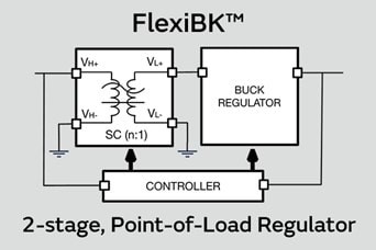
Murata’s power semiconductor FlexiBK™ PE241xx series is based on an ultra-high efficiency, 2-stage point-of-load regulator combining Murata-proprietary adiabatic or lossless charge pump technology. The technology is well suited to be applied from 2 or 3 cell battery or 12Vin point-of-load, providing step-down voltage conversion and significantly reducing the size/height of the solution while improving conversion efficiency. The IC is based on an integrated charge pump control architecture and integrated FET to configure a two-stage architecture consisting of a charge pump and a buck regulator. FlexiBK™ PE241xx series are available for evaluation kits.
The FlexiBK™ PE241xx series includes PE24101/PE24102, which supports an output channel with a maximum output current of 6A, an input voltage of 5.5V to 14.4V, and an output voltage of 0.6V to 2.0V with a switching frequency of 500 to 2000 kHz, 90% efficient, supports I2C interfaces, and is packaged with WLCSP. PE24101/PE24102 is equipped with ultra-thin and efficient 6A DC-DC MYTNA1R86RELA2RA and MYTNC1R86RELA2RA UltaBK converter modules. It adopts SMD package and supports PGOOD signal, over current protection, over-temperature protection, remote ON/OFF, output sensing, and other functions.
Murata’s another product, the FlexiBK™ PE24108, is a very small, low-profile, and ultra-high efficiency step-down DC-DC converter solution, an ultra-high efficiency, 3.3Vin, 9A, and 2-stage buck regulator IC that enables extremely low height and compact footprint through the use of innovative two-stage designs that combine capacitor divider charge pumps and dual phase buck regulators to provide an output current of 9A per stage over a wide input voltage range of 3V to 3.6V, with up to 4 phases in parallel to support 36A and 3.3V bus power supplies.
PE24108 output voltage is selected by external feedback resistors and can be adjusted by external AVS DAC to adjust between 0.37 and 0.7V for ultra-high efficiency and low-ripple performance for space-critical and noise-sensitive applications such as DSP/ASIC in optical modules or FPGA in networking equipment. PE24108 can be connected in parallel for applications with higher currents, typically optical modules, core supplies, ASIC, and FPGA.
Conclusion
Murata’s unique two-stage architecture for step down conversion is a highly flexible multi-stage architecture, including a combination of proprietary “pipeline” stage switched capacitor network (charge pump) and buck stage. Regardless of the conversion rate, it is almost lossless. Efficiency is largely independent of the difference between input and output voltages. It can greatly reduce the inductor size. Use low voltage FETs built on standard CMOS processes are used in the whole power supply system. Staggered charge pump operation can reduce ripple/EMI emissions and provide better transient performance. It will be one of the best options for power applications.
Courtesy: ARROW Electronics