


By Mark Patrick, Mouser Electronics
Data conversion is fundamental to our modern world, from smart sensors to smart home automation and power supplies. In this article, Mark Patrick, Mouser Electronics, explains how data conversion between the analogue and digital domains is achieved, and explores popular converter architectures. Equipped with this information, readers will have a better understanding of the technology and terminology, and the key datasheet specifications to review when selecting a device.


Converting analogue signals to digital signals and vice versa is essential in an increasingly connected world. We use analogue measurements to garner data about parameters such as temperature, humidity, and air pressure. But we need to convert these analogue signals for processing in the digital domain. Processing information digitally is a convenient, quick, and power-efficient process, for which low-cost microcontrollers are ideal.
Equally, we may need to convert digital signals into analogue signals. Indeed, some applications use both conversion methods: for example, in home automation systems. Analogue human speech is converted into a digital audio stream, which is then interpreted by a cloud-based machine learning algorithm. The answer or the desired music is then sent back to the speaker for conversion to the analogue domain. This is achieved using data converters.
Understanding data converters
Data converters are classified as either analogue to digital (ADC) or digital to analogue (DAC). A simple, functional block diagram of an industrial process closed loop controller featuring an ADC and a DAC is shown in Figure 1. Note that the input and output of the ADC and DAC are supported by signal conditioning functions. Signal conditioning may involve using low pass filters on the ADC input, for example, to remove any high-frequency signal artefacts that might interfere with the ADC’s conversion accuracy. Alternatively, signal conditioning may be applied to limit the input range of the acquired analogue signal to prevent damage to the ADC.
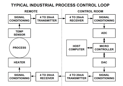
Figure 1: The use of an ADC and a DAC in an industrial process loop controller (Source: Analog Devices)
Where multiple analogue sensor elements are required, the input to the ADC can be multiplexed to provide a cost-efficient control circuit design. The design might require a programmable gain amplifier to accommodate different analogue input ranges from multiple sensors (Figure 2).
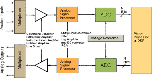
Figure 2: A complete analogue to digital to analogue control loop with a microcontroller or microprocessor (Source: Analog Devices)
ADC and DAC functions may be designed using a discrete component approach. However, the most time-efficient and PCB space-effective method is to select an integrated circuit (IC) that typically includes the ADC or DAC functions, a multiplexer, and some signal conditioning components.
The data conversion process
Data conversion essentially involves two distinct processes: sampling and quantisation. Sampling determines how faithfully the digital output signal represents the input analogue signal. It is typically quoted as the number of samples per second (s/s). A slow sampling rate is sufficient for slow-changing analogue signals, but a more rapidly changing input requires a faster sampling rate. On the far right of Figure 3, you can see that the analogue input signal is changing more quickly than the sampling rate, resulting in a loss of conversion accuracy.
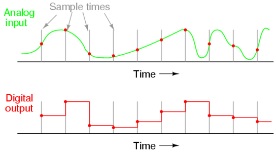
Figure 3: The impact of sampling rate on the reproduction of a digital output signal (Source: Kuphaldt – http://www.ibiblio.org/))
Quantisation determines the analogue value for each digital bit and the resolution of the ADC. For example, an 8-bit ADC can represent the input signal in 256 levels, but a 16-bit ADC improves the resolution to 65,536 steps, so each digital bit represents 256 analogue values compared to an 8-bit ADC. In general, the use case determines the selection criteria for the ADC’s resolution and sampling rate (Figure 4). Digital-to-analogue conversion uses the same principles of sampling and quantisation.
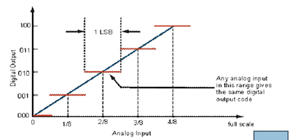
Figure 4: The quantisation process determines the value of each digital bit and the ADC’s resolution (Source Analog Devices)
Common converter architecture
ADC Architecture
The principal factors influencing ADC architecture are cost (simplicity of design), resolution, or linearity. Each use case will require different architecture attributes, but here are four of the most common.
A flash architecture converts an analogue signal into the digital domain using a parallel array of clocked comparators. Each comparator is fed with the input signal and a set fraction of a reference voltage from a resistor ladder (Figure 8). A flash architecture achieves conversion within one clock cycle, but it requires eight comparators for an 8-bit ADC, which also imposes a high input capacitance.
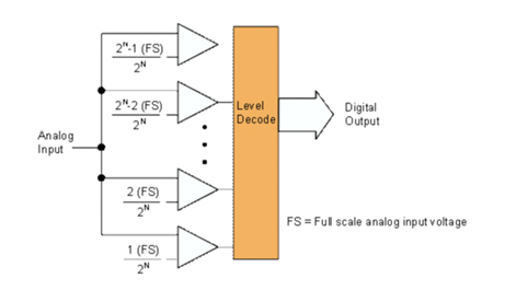
Figure 8: The outline architecture of a flash ADC (Source: Analog Devices)
A pipelined architecture typically uses a two-stage conversion process, each consisting of a sample and hold, a DAC, and an ADC. The first sample becomes the most significant bit (MSB). It is then fed back and subtracted from the input signal and the residual signal is sampled. This process is repeated for each bit from MSB to LSB. The pipeline model can accommodate a wide dynamic range of input signals and achieve a high resolution, but it is not as fast as a flash ADC and introduces conversion latency.
Successive approximation register (SAR) architecture compares the input signal against a known reference voltage, using successively smaller reference voltages for each digital bit (Figure 9). If the analogue input is greater than the reference, a bit is set. Otherwise, it remains at zero and continues to the next bit. SAR ADCs are compact because they only require a single comparator, and they have no pipelining delay. However, the DAC linearity and any comparator noise can affect accuracy.
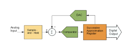
Figure 9: An outline of the SAR analogue-to-digital converter (Source: Analog Devices)
A sigma-delta architecture creates a sigma-delta modulator using an integrator, comparator, and a one-bit DAC (Figure 10). This modulator subtracts a value from the DAC and feeds the result to the integrator. The comparator converts the integrator output to a single-bit digital output, which is fed back to the input. This architecture yields a high resolution and can operate at a fast ‘oversampling’ rate.
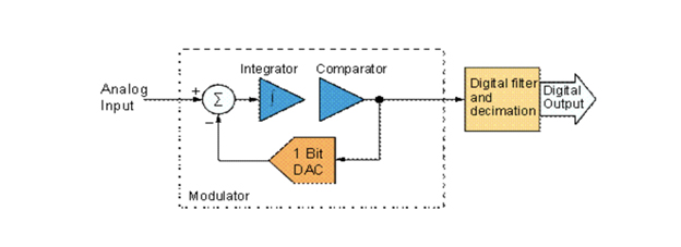
Figure 10: The architecture of a sigma-delta ADC (Source: Analog Devices)
Common DAC architecture
Typically, the simplest form of DAC uses string architecture. This deploys a string of precision resistors to create a voltage divider, converting a digital input to an analogue output (Figure 11). It can be prone to resistance-matching issues.
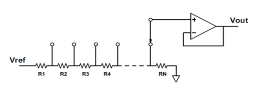
Figure 11: DAC binary-weighted string architecture (Source: Analog Devices)
An R-2R ladder architecture requires just two resistor values in a 2:1 ratio (Figure 12). This architecture suits voltage or current output configurations and avoids the resistance-matching problems associated with string architecture.
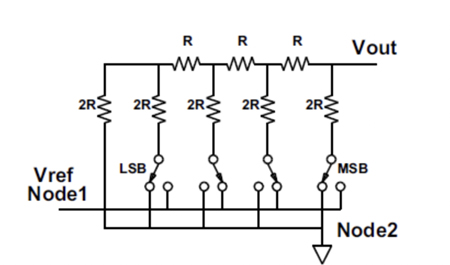
Figure 12: The basic architecture of an R-2R ladder DAC (Source: Analog Devices)
String and R-2R architectures use a fixed reference voltage and a fixed gain. However, the multiplying DAC (MDAC) architecture provides a digitally variable gain to a wide dynamic range analogue signal. It uses an R-2R ladder and a programmable gain op-amp. This gives the MDAC the ability to function as a DAC-based attenuator or amplifier and is ideally suited to high bandwidth AC or varying DC signals.
Conclusion
Data conversion is a key skill for engineers today, because it underpins so many of the automated systems on which our world relies. An understanding of popular converter architectures and the common terminology associated with data conversion will aid appropriate product selection.