


Chiplet technology is an older concept that has very recently gained prominence in the tech world.
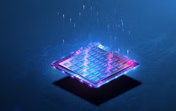
We are living in very promising times when it comes to the importance of semiconductor chips and technology innovations for the future of computing. Since the beginning of this decade, computing needs have multiplied greatly, mostly due to proliferation of data centers and the huge amount of data being generated and processed. Artificial Intelligence and Machine Learning are now used to process ever-increasing data which has led to servers significantly increasing their computing capacity. Servers have added many more CPU cores, have integrated larger GPUs used exclusively for ML, and have embedded custom ASIC AI accelerators or, FPGA based AI processing.


The evolution of newer and faster protocol standards is picking up speed as the industry keeps asking for higher performance. Chip integration is happening, with more transistors being added per sq. mm at every new technology node. In 1965, Intel’s co-founder, Gordon Moore made an informed prediction that approximately every decade, the size of transistors would shrink and the number of transistors on an electronic chip would double, consequently reducing the chip’s power consumption, manufacturing cost, and increasing its speed and capability. In 1975, he revised the period from a decade to just two years. This observation, famously known as Moore’s Law, has driven the electronics revolution of our modern age. However, there is now consensus in the industry that the focus on achieving Moore’s law is not valid anymore for advanced technology nodes.
Almost half a century later, the current electronic chips consist of billions of miniature transistors’ shrunken to just a few molecules photolithographically built on a Silicon wafer. While designers have been trying to squeeze out more density in recent years, it has come at a much higher cost of manufacturing devices on leading-edge process nodes and is taking much longer.
With the cost to manufacture an integrated chip steadily climbing and in particular a sharp increase in those costs in the latest generations due in part to increased mask layers, the industry can no longer rely on just engineering of smaller transistors to make computers more powerful. The literal physical limit has been reached on how small these transistors can be.
Instead of designing monolithic chips that incorporate all the important elements on a single silicon die, a new approach to IC design subdivides a system into functional circuit blocks called chiplets. A single chip is broken down into multiple smaller independent constituents that make up a chip built out of multiple smaller dies, connected together and combined in new ways. Chiplet technology is a key initiative to drive increased integration for the main SoC while using older nodes for other functionality.
The unique intellectual property blocks can be split across multiple chiplets, enabling products to be built with different configurations. If the product needs more, it simply adds in more of these chiplets. This same principle can be applied to memory channels, cores, media accelerators, AI accelerators, graphics, IO or anything else. The idea is that each IP can be split and then scaled up, meaning that the chiplets are tiny and can be built relatively quickly, while faults should be ironed out very quickly, too. In addition to saving space, this gives designers the freedom to glue together a wide variety of chiplets, as if assembling parts on a very small circuit board.
The goal is to mix and match which process nodes work best for different parts of the chip. With this manufacturing approach, high-performance ICs can be designed using the best transistor technology for the function. Fabrication cycles can be shorter and performance-wise chiplets can compete with monolithic circuits.
AMD
AMD’s Ryzen, Ryzen Threadripper and Epyc CPUs, which are based on the company’s Zen architecture, are examples of products that currently contain chiplets. The first-generation AMD EPYC processor was based on four chiplets. Each of these had 8 “Zen” CPU cores with 2 DDR4 memory channels and 32 PCIe lanes to meet performance goals. AMD had to work in some extra room for the Infinity Fabric interconnect across the four chiplets. These lessons were put to use with the second-generation 7nm Epyc processor.
AMD’s 3D chiplet technology combines chiplet architecture with 3D stacking. Earlier this year AMD showcased a new 3D chiplet architecture that will be used for future high-performance computing products set to debut. Using a hybrid bond approach that AMD says provides over 200 times the interconnect density of 2D chiplets and, again according to AMD, more than 15 times the density compared to existing 3D packaging solutions.
The first application of the 3D chiplet is called 3D vertical cache. To demonstrate the technology, AMD created a prototype by bonding a 3D vertical cache onto an AMD Ryzen 5000 series processor. AMD reported that the prototype Ryzen 5900X with 3D V-Cache attached delivered a 12 percent higher frame rate for Xbox Game Studios’ game “Gears 5.” In benchmarking on five other games, performance increased an average of 15 percent using the 3D V-Cache technology, according to AMD.
AMD has been packing multiple dies of Zen CPU cores and IO circuitry into individual processor packages, selling them as its Ryzen PC and Epyc server chips.
Intel
Intel’s next-generation 18A node will be ready for manufacturing in the second half of 2024, months ahead of the previously given 2025 timeline. Intel is now producing more 10nm wafers in a day than 14nm wafers. Intel’s next-generation Xeon Scalable server processor, called Sapphire Rapids, will be Intel’s first effort to fully embrace a chiplet architecture and it will be its first mainstream processor that supports DDR5 high-bandwidth memory, PCIe Gen. 5.0 and compute express link.
To scale up its data-center Sapphire Rapids chip to more cores, Intel had to split up the design into multiple dies. Set to launch in 2023, Sapphire Rapids’ compute tiles will have full access to cache, memory and input/output (I/O) functionality on all tiles. This means any one core will have access to all of the resources on the chip and are not limited to what’s built into the tile. Intel’s EMIB and Foveros 2D and 3D multi-die packaging tech will be at the heart of its Sapphire Rapids server CPUs and Ponte Vecchio accelerator GPUs. Intel’s ambitions for this packaging tech aren’t limited to its own silicon. The company is a founding member of the Universal Chiplet Interconnect Express (UCIe) consortium working to standardize the way chiplets from various vendors talk to one another. UCIe has already seen buy-in from some of the largest chipmakers and foundry operators, including TSMC and Samsung Electronics.
Intel’s 10nm process Alder Lake gaming chips, which combine performance processor cores for speed with efficiency cores for better battery life, is its 12th generation processor. Together with the company’s Raptor Lake (13th generation) and Meteor Lake (14th generation) processors, they represent Intel’s answer to increasingly competitive AMD processors.
While chiplets do provide the industry with a compelling solution, for most companies that shift will happen slowly until proven standards are in place. Interoperability and compatibility depend on many layers and segments of the supply chain coming to agreement. With the flooding of ideas, work needs to be done on the design, verification, and modeling end, and testing needs to happen continually throughout product life cycles. Moreover, everything needs to be reviewed and updated regularly as algorithms change, and because devices within a package may age and degrade at different rates.
The number of transistors on a chip and the latency of their communication links decide the speed, cost, capabilities, and power consumption of the chip, thereby determining the performance and affordability of the electronic gadgets that use the chip. Chiplet strategies rely on complex high-speed interconnect protocols. What is more, communications between chiplets costs more power than a monolithic interpretation, and usually means higher latency. But the benefits afforded from using the right process at the right time are significant, as it helps provide both performance and power.
Data-centric applications are now the driver of the electronic industry, and these applications demand increasing bandwidth, computing power, and ultimately require more transistors. Chiplet-based architectures will be the solution to deliver ever-increasing processing capabilities and ultimately more transistors in a single package.