

High-quality data transmission, high-precision information sensing, and high-sensitivity signal detection are important means to achieve precise perception and effective identification. High-performance chips, terahertz transmission T/R components, and extreme environment sensor manufacturing technologies have become key frontier research hotspots. Its effective implementation strongly depends on the ultra-precision micro-nano manufacturing level of the complex microstructure of core functional devices. As an excellent carrier for information-enabled core functional devices, pure copper metal has ultra-high electrical conductivity, thermal conductivity, and high ductility, as well as low-loss signal transmission capabilities. Therefore, it has received extensive attention in the field of micro-nano manufacturing.
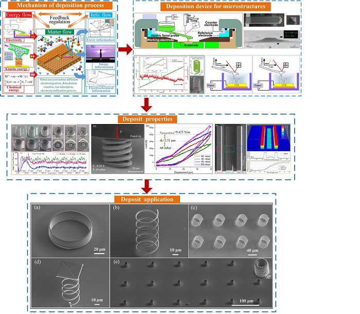
Recently, Prof. Huadong Yu, Researcher Jinkai Xu, Wanfei Ren, Zhongxu Lian, Xiaoqing Sun, and Zhenming Xu from Changchun University of Science and Technology have written an article “Localized Electrodeposition Micro Additive Manufacturing of Pure Copper Microstructures”


The researchers systematically introduced the localized progress of the micro-additive material manufacturing method of the micro pure copper structure and improved the manufactured microstructure for performance testing.
Professor Huadong Yu (a professor of Jilin University, and the chief technology officer of Key Laboratory of Cross-scale Micro-Nano Manufacturing of Ministry of Education), Jinkai Xu ( a professor of CUST and the director of the National and Local Joint Engineering Laboratory of Precision Manufacturing, and Detecting Technology/Key Laboratory of Cross-scale Micro-Nano Manufacturing of the Ministry of Education, and the leader of the micro-nano manufacturing discipline of CUST.), and Wanfei Ren (a lecturer of CUST) have developed a few methods for manufacturing of microstructures. The details are as follows:
“Although the technique demonstrates the fabrication of pure copper microstructures, the technology has applications as early as 2018.
a mathematical model of the synergy of pulsed micro-jet, focusing electric induction and atomic force servo. Although preliminary, this model establishes the initial model of electrochemical deposition, material transport, and force information feedback.”
“The article mainly introduces the various characteristics of the deposited pure copper microstructure. Can you briefly introduce it?”
“The manufacture of pure copper microstructure was realized, and the deposition rate was 0.887μm/s. Shear modulus of pure copper microspring was tested and reached 60.8GPa.”
“What is the role of the device during the experiment?”
“The device used in the experiment is from Exaddon AG, Switzerland. The function of the device is to monitor the state of the deposition process during the experiment. Thanks to the device, the Z-direction position of the atomic force probe and the bending state of the cantilever can be detected online at the same time.”