

In yesteryears, chip packaging was an afterthought. Chipmakers were more focused and worried about IC design. Semiconductor Packaging was considered a mere commodity, which was simply used to house the design, but times have changed significantly and there are several reasons for that. 5nm node, 3nm node, and 2nm node are currently on the horizon, and researchers and designers have no intentions to stop, in fact, they are aiming for the limitless miniaturization of components.
Packaging is an essential part of semiconductor manufacturing and design. It affects power, performance, and cost on a macro level, and the basic functionality of all chips on a micro-level.


Many types of packages are in use today and more are either in research at universities or ready for production — everything from the complex stacked die with through-silicon via to fan-outs and complex systems on-chip. Packages come in different materials, can be standard or custom, and can have active or passive cooling.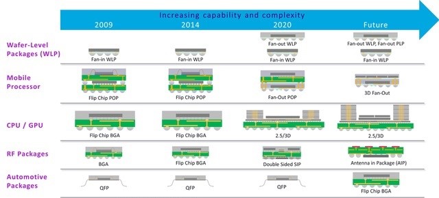 Materials, and the science of materials, are what have enabled the semiconductor industry to progress from the first integrated circuits to the most complex systems on chips and processors that are being manufactured today.
While many materials have been suggested for chips over the past few decades, the predominant ones have been variations of silicon, in large part because the process has been so well tested and proven that it is hard to justify replacing it from a cost and yield perspective. Likewise, interconnects are large copper.
Comprehensive Semiconductor Packaging Materials Spanning the Gamut
Besides silicon, a host of other materials have been included in semiconductors, ranging from thin films to improve or retard the flow of electrons through channels in the chip, oxides (low k and high k) to improve signal integrity by providing a buffer between tightly packed wires,
As the leading edge of design creeps forward, though, much consideration is being given to different materials at every step of the design and manufacturing process in an effort to minimize current leakage, quantum effects, and the electrical and physical effects from thinner wires, smaller features, and more complex signal routing.
Organics substrates, Leadframes, Mold Compounds, Underfill materials, Bonding wire, Liquid encapsulants, Solder balls, Wafer level package dielectrics, Thermal interface materials, Die attach materials are some of the typically used Semiconductor packaging materials.
To have a better understanding of the subject, ELE Times Sub Editor and Technical correspondent Mayank Vashisht, was fortunate enough to have a profound conversation with an industry expert of the subject matter, Sreeram N S, Technologist, Interface Products, Texas Instruments India.
To begin with, Sreeram reflected upon the ever-increasing importance of an activity which was considered as a background operation not so long ago, and what led to this change over the years.
“In the initial days, packaging would simply be a means of boxing the silicon for electrical connectivity. However, the increasing demand for capability and requirements in terms of speed, power, functionality, and usage in harsh environments, has driven the need for advancements in IC packaging.”
To understand it better, Sreeram cited an example, “package parasitics began impacting signal integrity, materials and poor thermal conductivity limited temperature range, and an I/O count increase to offer more functionality and speed was not possible. Furthermore, as ‘IC design’ progressed with exponential scaling in order to provide higher performance, IC packaging required to be able to do more with Moore.”
He further added, “Thanks to advancements in the industry, semiconductor packaging has continuously evolved over the years. New trends in IC packaging enable better ways of integrating silicon solutions into the complete system-in-package. Today, as electronics are needed everywhere, advanced packaging is becoming a more viable option to facilitate new solutions, while meeting performance and cost requirements across Personal, Automotive, Industrial, Medical, Aerospace, and Defense electronics.”
Sreeram also helped me understand the degree of efficiency of the advanced form of heterogeneous integration, spanning up to 2.5D/3D, fan-out, and system-in-package in comparison to the traditional ways of packaging. “Both serve different purposes and different levels of flexibility for system designs.”
He added, “Traditional packages are building block ICs that provide increased flexibility, whereas the advanced packages enable single-chip solutions, reduce system design complexities and solution size, and enable new solutions.
Furthermore, advanced packaging pushes the entitlement of silicon and helps meet application requirements such as high reliability in aerospace, robustness in harsh operating conditions like factory environments, high EMC in automotive electronics, etc. Also, it provides several options to choose from depending on system design trade-offs for cost and performance, like leaded, unleaded, Ball Grid Array (BGA), Wafer Chip Scale Package (WCSP), to name a few.
A few notable examples of advanced packaging techniques are crystal-less MCUs with integrated BAW resonators, galvanic isolators with integrated magnetics for power and signal isolation, enabling robust single-chip solutions. These advancements allow current and future generation ICs that are more efficient and reliable while offering higher performance and reducing system costs.”
During our conversation, we also touched upon the advanced packaging tends to grab the headlines and is making inroads, and, yet wire-bond and flip-chip are still widely used today. “Advanced and traditional packaging are two ends of the spectrum with equal focus. One end brings advanced IC packaging techniques to enable new solutions, as well as capabilities to meet performance requirements. Wire-bond and Flip-chip on the other hand continues to provide building block ICs for system design flexibility, at a lower cost, making semiconductors more affordable”, said Sreeram.
He further added, “Advancement in IC packaging techniques combined with the simplicity of wire-bond and flip-chip packages have enabled IC manufacturers to continuously push boundaries. This has helped reduce cost by minimizing BOM and increasing assembly line throughput by using copper bond wires, high-density lead frames, stamp tools, etc. These simple packages offer higher levels of reliability than complex packages, which is also one of the reasons why these packages are widely used in system designs even today.”
Exclusive Inputs –

Mayank Vashisht | Sub Editor | ELE Times