By Steven Keeping, Digikey
Gigabit Ethernet (GbE) is a robust, high-speed communication system in widespread use across domestic, commercial, and industrial premises. However, Ethernet systems do present challenges, particularly when connectivity extends beyond the building. Extended lines can be subject to unexpected high-level transient voltages and currents, and electrostatic discharges (ESD) are an ongoing risk.
The GbE physical layer (PHY) does include some components that provide a degree of protection, such as the isolation transformer. But the built-in transient voltage mitigation can’t be relied on to offer protection in all circumstances.
Transient voltage suppression (TVS) diodes are a proven, inexpensive, and robust circuit protection device in space and cost-constrained applications such as GbE. Under normal operation, the devices appear transparent. Yet the devices must protect multiple communication channels from surge currents up to 40 amps (A) and ESDs up to 30 kilovolts (kV), and maintain low loading capacitance in normal use to ensure high-speed signal integrity.
This article describes the design challenges presented by GbE high-voltage transient and ESD protection, and then considers the unique characteristics of TVS diodes required for energy suppression. The article then describes some commercial solutions for the problem before showing how to design the selected devices into systems for transient protection to standards such as IEC 61000-4-2, -4, and -5.
The dangers posed by transient voltage effects
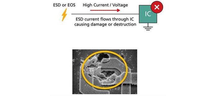
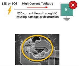
GbE is a wired high-speed communication system. Copper connections carry the differential signals that represent the “zeros” and “ones” making up the digital signal stream. However, that copper wire is also the perfect transport mechanism for high transient voltages and ESD events that could damage silicon circuit elements (Figure 1).
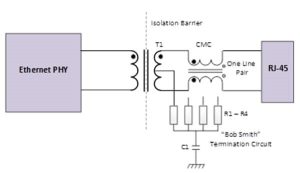
The design of the GbE PHY includes some degree of protection through the isolation transformer. The GbE specification (IEEE 802.3) calls for a minimum isolation rating of 2.1 kV. Most commercial transformers offer 4 to 8 kV isolation. Furthermore, GbE interfaces typically include a common mode choke (CMC), an inductor used to block higher-frequency AC to help reduce ESD spikes. A final degree of protection comes from the “Bob Smith” termination. This uses a 75-ohm (Ω) resistor to implement a common-mode impedance match for signal pairs collectively connected via a capacitor to ground. The termination can help reduce the common-mode emissions discussed later (Figure 2).
Simply relying on the GbE PHY isolation transformer, the CMC, and the termination circuit for comprehensive protection is risky. While the components offer some transient voltage mitigation, there are several circumstances that leave the port exposed to damage.
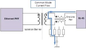
GbE transient voltage excursions can be classified into either common or differential-mode in nature. During a common-mode voltage transient, all the GbE PHY conductors instantaneously rise to the same voltage with respect to ground. Because all conductors are at the same potential, there is no current transfer from one conductor to another. Instead, current flows through to ground. A common path for current flow is through the conductor to ground via the transformer center tap and through the termination circuit (Figure 3).
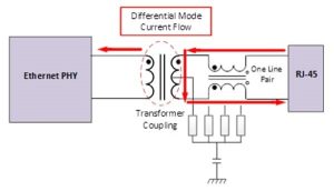
The differential-mode surge is different. Current flows into the GbE port on one signal line of the differential pair, through the transformer, and back out of the port on the other signal line. The transient current flowing through the transformer’s primary winding induces a current surge in the secondary winding. Once the surge is removed, the stored energy in the transformer will transfer to where the fragile GbE PHY is located. It is this transferred energy that, at best, results in lost data and glitches and, at worst, leads to permanent damage (Figure 4).
Figure 4 shows that the differential-mode surge is the most dangerous as it is the one that exposes the GbE PHY to potentially damaging voltages. Additional protection is needed on the secondary side of the isolating transformer to protect against these surges.
Using TVS diodes for surge protection
Protection of the GbE PHY requires devices that can isolate, block or suppress the large transient energy pulses. Additional transformers can fully isolate Ethernet electronics but are bulky and can be expensive. Fuses are an inexpensive method of blocking but must be reset or replaced after every trip event. TVS diodes are a good compromise; they effectively suppress the peak transient voltage to a safe level, don’t require resetting, are compact, and are reasonably priced.
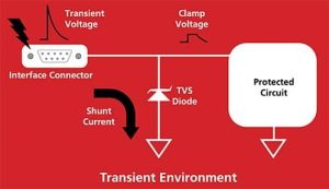
Structurally, a TVS diode is a p–n device specifically designed with a large junction cross-sectional area to absorb high transient currents and voltages. While the voltage/current characteristics of a TVS diode are similar to a zener diode, the devices are designed for voltage suppression rather than voltage regulation. A key advantage of a TVS diode is its rapid response (typically within nanoseconds) to electrical transients—diverting the energy of the transient safely to ground while maintaining a constant “clamping” voltage—compared to other suppression devices (Figure 5).
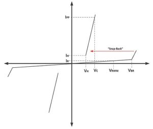
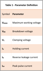
During normal operation, the TVS diode presents a high impedance to the circuit for voltages up to its working voltage (VRWM). When the voltage across the device terminals exceeds the breakdown voltage (VBR), avalanche breakdown occurs in the diode’s junction causing it to “snap-back” or switch to a low-impedance on-state. This lowers the voltage to a clamped level (VC) as the transient peak pulse current (IPP) flows through the device. The maximum voltage to which the protected circuit is subject is equal to VC and is typically modest. Once the current decreases below the holding current (IH), the TVS diode returns to a high-impedance off-state (Figure 6 and Table 1).
TVS diodes from reputable manufacturers are designed to protect interfaces while meeting tough immunity standards detailed in documents such as IEC 61000-4-2 (ESD), IEC 61000-4-4 (EFT), and IEC 61000-4-5 (lightning).
IEC 61000-4-5, which specifies how to test for surge immunity, provides details of the typical surge waveform used to determine a TVS diode’s capability. The waveform simulates an indirect lighting strike and reaches 90 percent of its peak current value (tp) in 8 microseconds (µs) and decays to 50 percent of its peak value in 20 µs. Datasheets often refer to this as the “8/20 µs waveform”, and provide details of the waveform’s maximum peak pulse current (IPP) which the protection device can withstand. Datasheets also typically detail the product’s response to the associated voltage surge waveform caused by an indirect lighting strike of 1.2/50 µs (a transient surge reaching its peak voltage in 1.2 µs and decaying to 50 percent of its peak value in 50 µs).
The other key protection characteristic of a TVS diode is its “ESD withstand voltage”. This is the maximum static electricity discharge voltage that the protection device can tolerate without damage and is typically of the order of tens of kV.
TVS diodes for GbE PHY protection
In addition to GbE, TVS diodes are available for the protection of a range of interfaces, including HDMI, USB Type-C, RS-485, and DisplayPort. But each of these interfaces demands subtly different levels of protection. That makes it important that the TVS diode be designed for the specific application.
Semtech, for example, makes a range of TVS diodes targeted at GbE interface protection. The devices are manufactured using a process technology that Semtech says results in reductions in leakage current and capacitance relative to other silicon-avalanche diode processes. A further advantage of the product range is that it features a low operating voltage from 3.3 to 5 volts (depending on the version) to save energy.
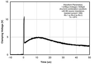
For example, the RailClamp series includes the RCLAMP0512TQTCT which is suitable for 2.5 GbE interface protection. This device features an IPP capability of 20 amperes (A) (tp = 8/20 and 1.2/50 µs) and a peak pulse power (PPK) of 170 watts. The ESD withstand voltage is +/-30 kV. The VBR is 9.2 volts (typ), IH is 150 milliamps (mA) (typ), and VC is 5 volts typical and 8.5 volts maximum (Figure 7).
The RCLAMP0512TQ is a compact device in a 3-pin SGP1006N3T package that measures 1.0 x 0.6 x 0.4 millimeters (mm).
There are other products in the Semtech RailClamp series that offer greater protection for 1 GbE applications used in potentially more hazardous situations. The RCLAMP3374N.TCT, for example, features an IPP capability of 40 A (tp = 8/20 and 1.2/50 µs) and a PPK of 1 kilowatt (kW). The ESD withstand voltage is +/-30 kV. VC is 25 volts (max) when IPP = 40 A. The component measures 3.0 x 2.0 x 0.60 mm.
The mid-range device in the RailClamp range is the RCLAMP3354S.TCT. This is suitable for 1 GbE protection and offers an IPP capability of 25 A (tp = 8/20 and 1.2/50 µs) and a PPK of 400 watts. The ESD withstand voltage is +/-30 kV. VC is 16 volts (max) when IPP = 25 A.
Designing in TVS diode protection
Figure 8 shows a GbE PHY protection scheme using the RCLAMP0512TQTCT. The devices are located on the PHY side of the transformer to protect against differential-mode surges, with one device placed across each Ethernet line pair. The Ethernet differential pairs are routed through each TVS diode component at Pins 1 and 2, with Pin 3 not connected.
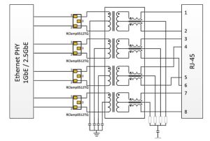
The engineer should limit parasitic inductance in the protection path by locating the protection component as physically close to the Ethernet PHY magnetics as possible, and preferably on the same side of the printed circuit board (pc board). It also helps if ground connections are made directly to the pc board ground plane using microvias.
The reduction of parasitic inductance is especially important for suppressing fast rise time transients. Inductance in the path of the protection device increases the VC to which the protected device is exposed. VC is proportional to the path inductance times the rate of change of current during the surge. For example, just 1 nanohenry (nH) of path inductance can increase the peak VC by 30 volts for a 30 A ESD pulse with a 1 nanosecond (ns) rise time.
Note that the selected Ethernet transformer will be required to survive anticipated surges without failure. A typical Ethernet transformer can withstand a few hundred amperes (tp = 8/20 µs) before failure occurs, but this needs to be verified by testing. Alternatively, if the surge immunity of the transformer is suspect, the protection component can be placed on the line side of the transformer. The downside is that the additional protection afforded by the transformer is then lost, and the ability of the GbE system to withstand high energy surges is limited to just the capability of the protection device.
Conclusion
GbE is a reliable and widespread high-speed communication system, but all systems using conductors are subject to energy transients due to phenomena such as lightning and ESD. Such surges are mitigated to some extent by the GbE port’s transformer, CMC, and termination circuit, but differential-mode surges can bypass this suppression and damage the Ethernet PHY. Additional protection is recommended for critical systems.
TVS diodes are a good option because they effectively suppress the peak transient voltage to a safe level, don’t require resetting, and are compact and mid-priced. Careful matching of the protection component to the application is advised, as they are available in a wide range of capabilities, including peak current protection. Additionally, adherence to good design guidelines, such as position and grounding, is recommended to maximize the protection of a given TVS diode.


