


While RF circuits might appear complex at first glance, with the right tools, you can incorporate RF designs into your PCB projects effortlessly and confidently.
This blog post will delve deep into the AWR Microwave Office to Allegro RF Design flow. The foundation of this design flow is Cadence Unified Library, which is used to exchange data between AWR Microwave Office and Allegro PCB Design applications. Cadence Unified Library contains all the necessary information to design an RF schematic and a layout in AWR Microwave Office, including PCB technology, manufacturable components, and vias. AWR Process Design Kit (PDK) is generated from Cadence Unified Library and used by AWR Microwave Office to capture the RF schematic and the layout. The RF design is exported as a single container (.asc) file from AWR Microwave Office.


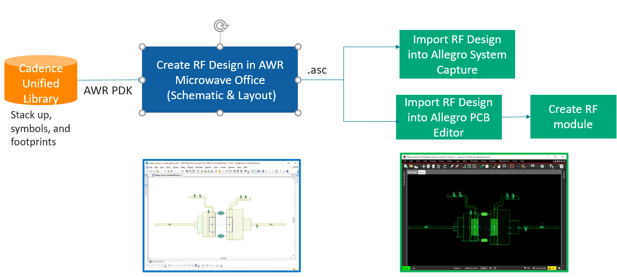
Let’s go through the design flow tasks to bring an RF design created in AWR Microwave Office into Allegro System Capture and Allegro PCB Editor and reuse these RF designs.
Importing RF Design into Allegro System Capture
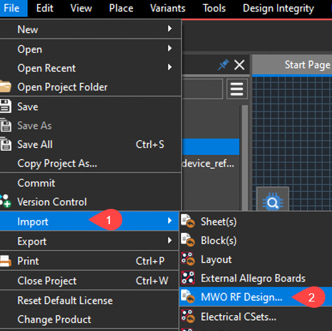
To import an RF design in Allegro System Capture, do the following:
- Choose File – Import – MWO RF Design.
- In the file browser that opens, browse to the location of the .asc file exported from AWR Microwave Office.
The RF design is imported as a block that can be used to create schematic blocks in Allegro System Capture.
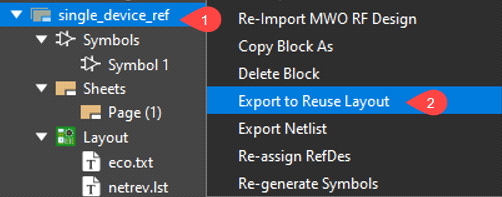
To mark the block as a reuse block, do the following:
- Select the RF block, right-click, and choose Export to Reuse Layout.
- In the Options form, specify the input layout field value to the path of the board file used for generating Cadence Unified Library.
After the export process is completed, a new board file is generated with connectivity information.
Importing RF Design into Allegro PCB Editor
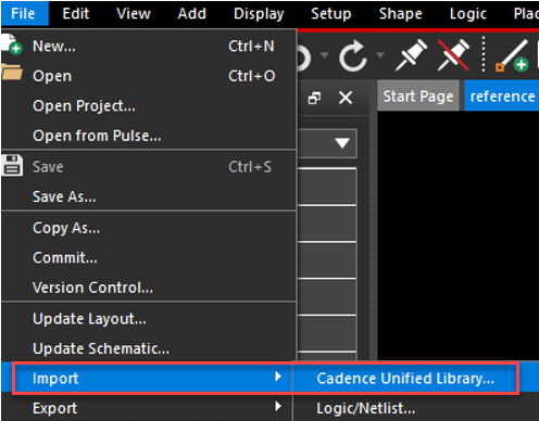
To import the RF design into the layout design, perform the following steps in Allegro PCB Editor:
- Open the board created in the previous step.
- Choose File – Import – Cadence Unified Library.
After the import process is completed, the RF layout is placed in the design canvas.
Creating RF Design Module
Saving the RF layout as a module helps you create multiple PCB designs with the same RF logic. To create a module in Allegro PCB Editor, do the following:
- Choose the Tools – Create Module menu command.
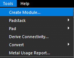
- Select the entire RF layout intended for inclusion in the module by drawing a rectangular boundary, then click anywhere on the design canvas.
- Specify a name in the Save As file browser and click Save to save the module (.mdd) file.
Reusing RF Blocks in Existing PCB Designs
If marked for physical and logical reuse, the RF block can be instantiated as a reused RF block in an existing schematic design. When this schematic design is transferred to Allegro PCB Editor, the RF modules can be reused in a larger PCB. To instantiate the RF blocks in an existing schematic project, perform the following:
- Right-click the RF block name in Allegro System Capture and choose Place as Schematic Block.
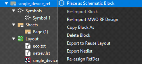
The packaging options appear when you place the block.
- Select the Physical Reuse Block check box. This step is essential to link the schematic to the reuse RF module.
- Repeat the above steps to place multiple instances of the RF Block.
- Complete the schematic design.
- Use the Export to Layout option to complete the packaging process.
Conclusion
The tightly integrated AWR Microwave Office-Allegro PCB solution is a step ahead of the traditional flows in ensuring a first-time-right verification and manufacturing of RF modules in the context of a real PCB. The key value lies in a shift left approach where the RF section is designed using real manufacturing parts and PCB technology, thereby eliminating the recapture and verification of the RF block in the later stages of the PCB design process.